This article discloses that “Japan’s Semiconductor Strategy 2024+1/2—NVIDIA and AI Chip Companies” will be available for purchase from November 19, 2024.
[About this book]
This book provides a detailed explanation of the trends toward the revival of Japan’s semiconductor manufacturing industry, the essence of the leadership of NVIDIA leader Jensen Hwang, and the latest trends of AI chip companies challenging NVIDIA. This is a must-have guidebook for anyone who wants to ride the wave of AI semiconductor technology innovation. Please take a look.
[Features of the content]
The global AI semiconductor industry is in the midst of unprecedented innovation. This book combines the latest information and in-depth analysis to deliver a total of 492 pages of rich content. This volume reflects the historic turning point of the Japanese semiconductor industry, which is shifting from vertical integration to horizontal division of labor.
[Page structure]
This book covers the latest topics in the AI semiconductor industry as follows:
– Japan’s semiconductor strategy: 200 pages (Japan’s manufacturing capabilities and its future reevaluated from the perspective of the global market)
– NVIDIA’s innovation and leadership: 180 pages (NVIDIA’s leadership challenges and secrets to success)
– AI chip market competition: 80 pages (Strategies and possibilities of emerging companies challenging NVIDIA in the next-generation AI chip market)
[Store sales]
Available at major bookstores in urban areas, such as Shosen Book Tower.
[General bookstores]
You can order from your local bookstore through Nishimura Shoten (TEL: 03-5879-7681), a distributor specializing in academic books.
[Publisher web store]
[Amazon]
[Recommended points]
– Thorough explanation of Japan’s semiconductor strategy: A unique analysis of the technical challenges facing Lapidus’ 2nm process challenge and the position of Japan’s semiconductor industry in the global market.
– Envisioning the future of AI and semiconductors: Explore the process of a new industrial revolution in the 21st century brought about by NVIDIA’s technological innovation and co-creation model.
– Comprehensive information for investors and policymakers: We provide information that will be useful for decision-making, covering trends in semiconductor-related stocks and details of government support measures.
– Latest information for career development: We cover the latest technologies and trends required in the semiconductor industry and provide hints for opening up the future.
[Contents]
– Growth potential and market trends of 2nm chip manufacturing: We delve deeper into the challenges and prospects of next-generation chip manufacturing technology, which is attracting attention from the public.
– The evolution of NVIDIA’s AI chips and CUDA platform: We provide a detailed explanation of NVIDIA’s unique ecosystem supported by 20 years of technological innovation.
– Jensen Hwang’s leadership and management philosophy: We analyze the secret to the success of NVIDIA’s CEO, who is leading the semiconductor industry.
– New competitive trends in the AI market: AMD and 15 other startups are taking on innovative AI technology and the market potential.
– Outlook for international cooperation and technological innovation: Global collaboration centered on NVIDIA and Rapidus and its future vision.
– Measures to deal with geopolitical risks: We explain the impact of the US-China conflict on the semiconductor industry and strategies to overcome these risks.
[Explanation of each chapter]
● Chapter 1 “Japan’s semiconductor strategy and Rapidus: Integrating diplomacy, security, and economic policies”
This chapter explains why Japan is strategically promoting the development of next-generation semiconductors. It comprehensively covers the latest government announcements regarding Japan’s semiconductor strategy. In particular, it focuses on the “successful chances” of Japanese semiconductor manufacturing, centered on Rapidus, and contains as much information as possible that the public wants to know. If successful, the “leap-frog” strategy of Japanese semiconductor manufacturing will be a great opportunity to regain international competitiveness in one fell swoop. As the background to working on 2nm technology, it explains competitive advantages and the effects of introducing new technologies (GAA transistors, EUV lithography, backside power supply, etc.).
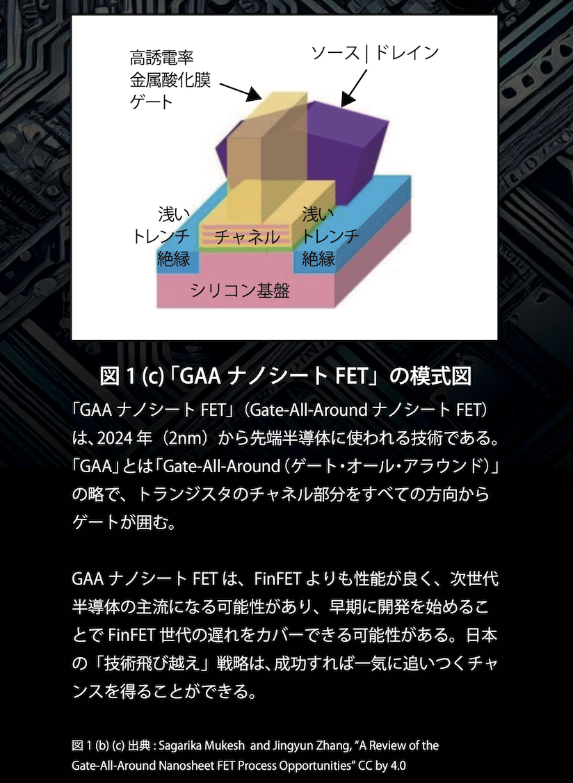
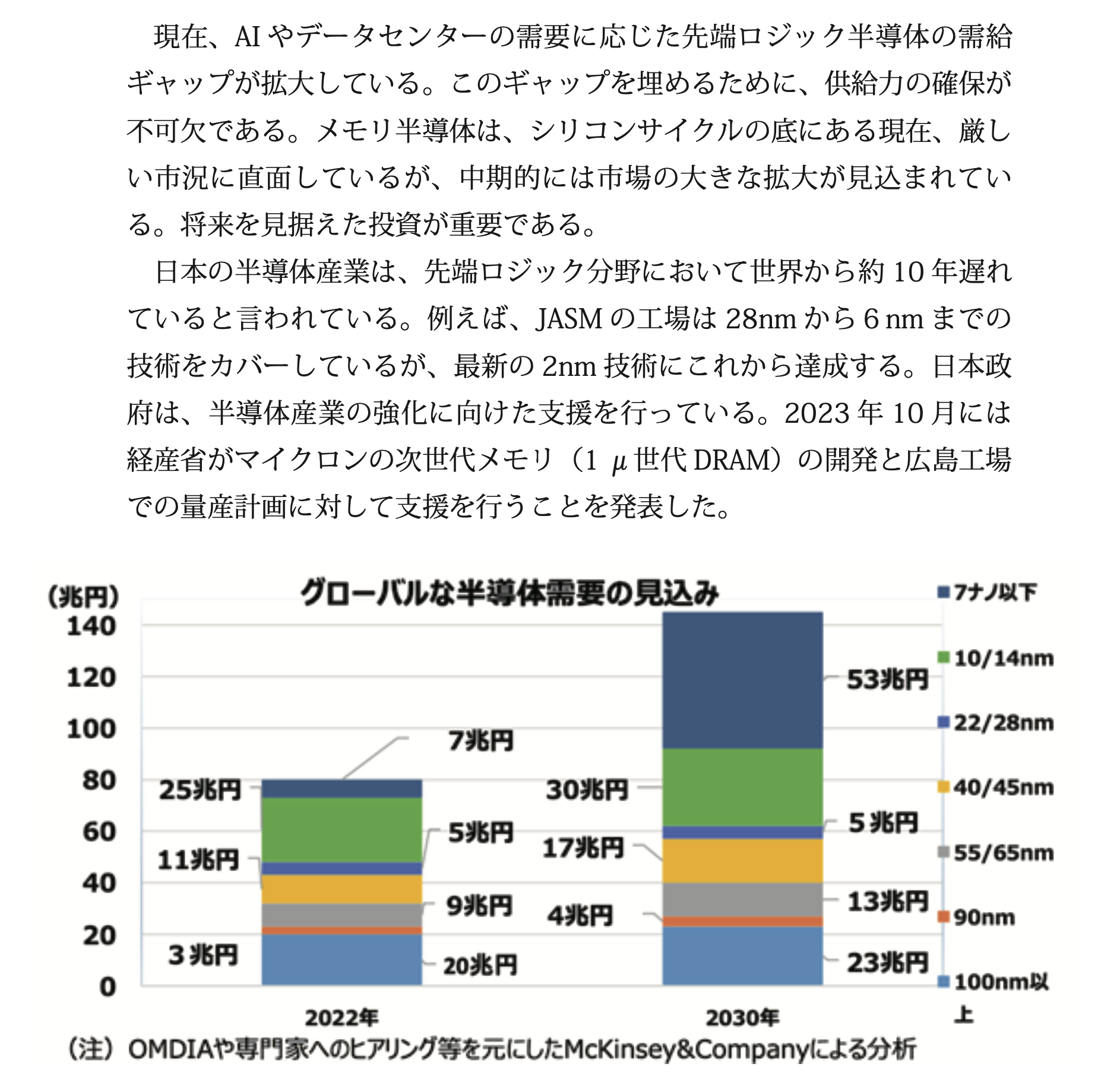
Japan’s semiconductor manufacturing strategy is centered on the development of 2nm technology, aiming to innovate through the introduction of new technologies (such as GAA transistors, EUV lithography, and backside power supply) while ensuring competitive advantage. In light of the history of the semiconductor industry and the evolution of MOSFET technology, the strategy emphasizes the importance of next-generation technology groups (such as 3D stacking technology and chiplet design) and compares and examines the 2nm roadmaps of various countries such as TSMC, Samsung, and Intel. It also touches on the progress and challenges of Japan’s own 2nm fab by Rapidus, and organizes the roles of key players that make up the supply chain, such as EDA and foundries. In addition, it explores use cases for AI computing and next-generation memory, and promotes research and development and human resource development through the Leading Semiconductor Technology Center (LSTC). With an approach that integrates diplomacy, security, and economic policies, Japan is strengthening its strategic positioning in the US-China competition while placing emphasis on financial sustainability and spillover effects on the regional economy.
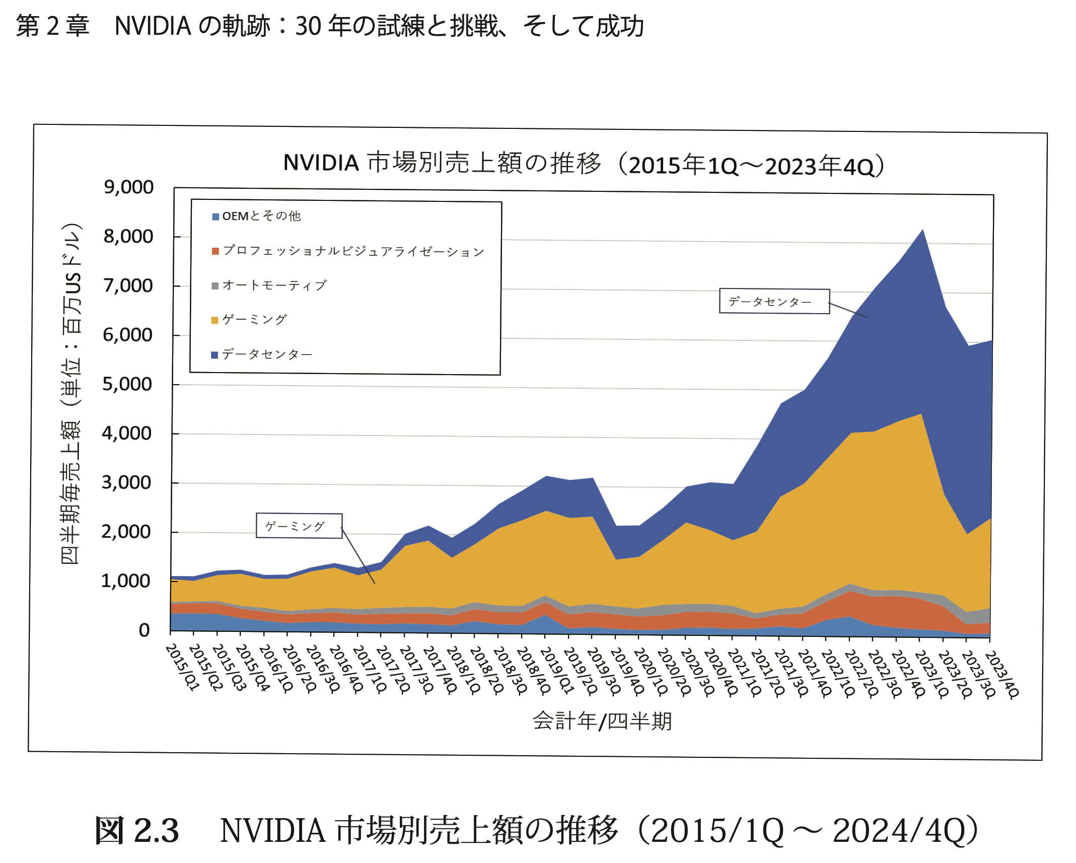
● Chapter 2 “NVIDIA’s Trajectory: 30 Years of Trials, Challenges, and Success”
In this chapter, we analyze the actual state of NVIDIA by visualizing information such as the scale of its actual business and application fields based on financial documents released by NVIDIA since its founding. We have compiled NVIDIA’s management data over the past 30 years, focusing on revenue growth, expansion of its share in the GPU market, and the evolution of semiconductors for AI data centers. We have summarized the sales by application for each year when NVIDIA won the competition in the desktop PC GPU market and strengthened its revenue base with AI products. TSMC (Taiwan Semiconductor Manufacturing Co., Ltd.) is an important partner that supported NVIDIA’s success. Founded in 1987, TSMC adopted a pure-play foundry model and built its competitiveness in the global semiconductor industry. Through close cooperation with TSMC, NVIDIA has succeeded in realizing advanced semiconductor technology and achieving economic results.
● Chapter 3: Graphics and AI Revolution: Jensen Fan and NVIDIA’s Challenge
This chapter analyzes NVIDIA’s 30-year history from its founding to the present from various angles, including leadership, product development, market strategy, technological innovation, and the AI revolution. To provide the necessary clues to understand Jensen Fan, I also devoted pages to episodes of my direct contact with Jensen from 1994 to 2000 and from 2005 to 2006.

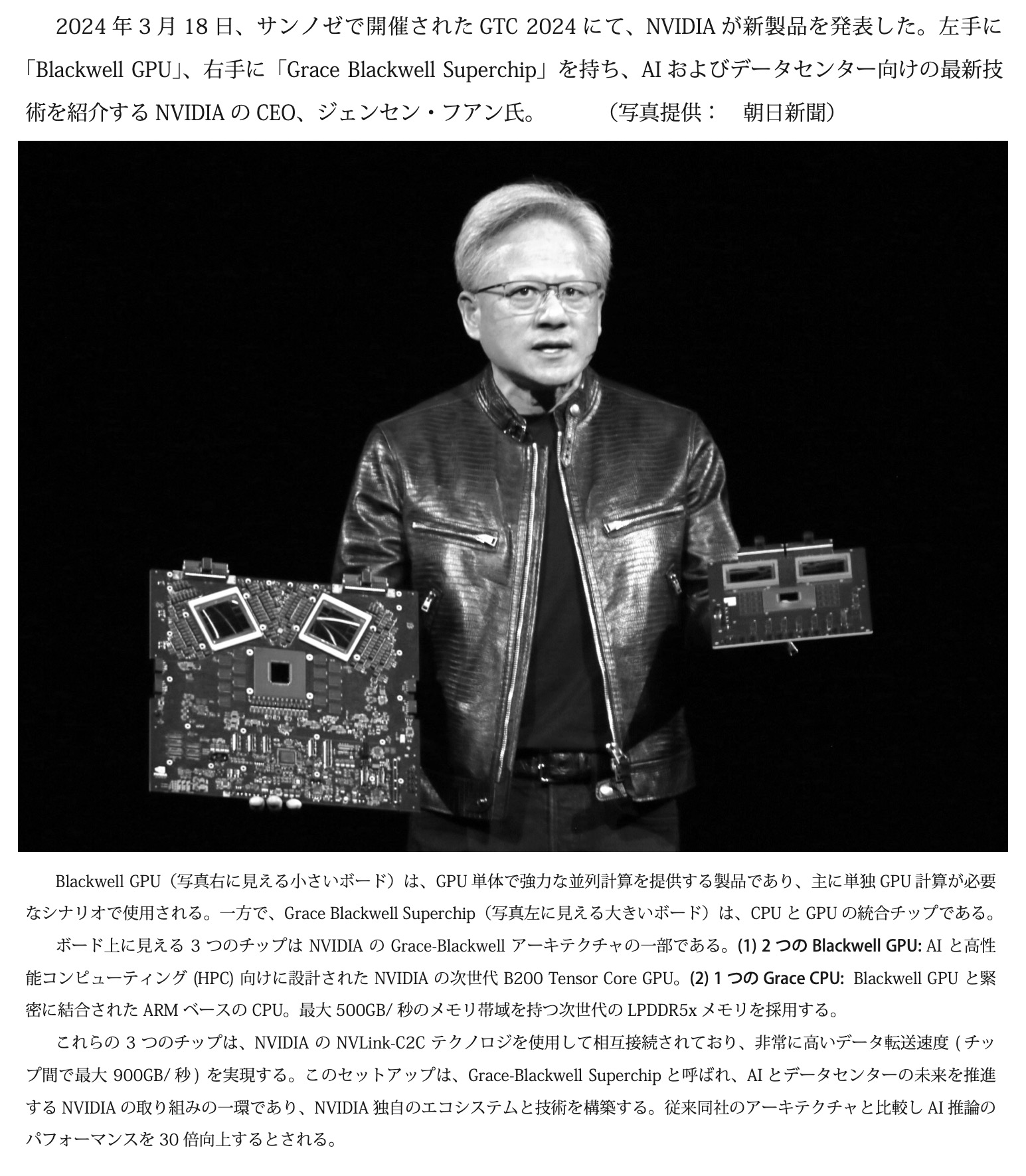
Jensen Huang said that since its founding in 1993, Jensen initially focused on the 3D graphics market, and experienced waves of rapid growth and stagnation. In 2006, however, he launched Operation Barracuda at NVIDIA, which aimed to gradually shift Intel CPU workloads (processing contents) to GPUs (graphics processing units). By replacing workloads processed by CPUs with GPUs over a period of more than 10 years, PCs have become more powerful, and in order to increase the importance of NVIDIA GPUs in PCs, he decided to continue developing a general-purpose GPU software development tool environment called CUDA. Since then, NVIDIA has continued to develop new market opportunities through CUDA, and the research and development of Geoffrey Hinton, who won the Nobel Prize this year, used CUDA, which led to NVIDIA’s great success in the AI market, and NVIDIA’s presence in fields such as generative AI is also increasing. NVIDIA’s innovations, which began with Operation Barracuda and the development of CUDA, have revolutionized the direction of computer architecture across the industry. In recent years, NVIDIA has become the world’s largest company through its AI innovations, and CEO Jensen Huang has risen to the top of the economic world.
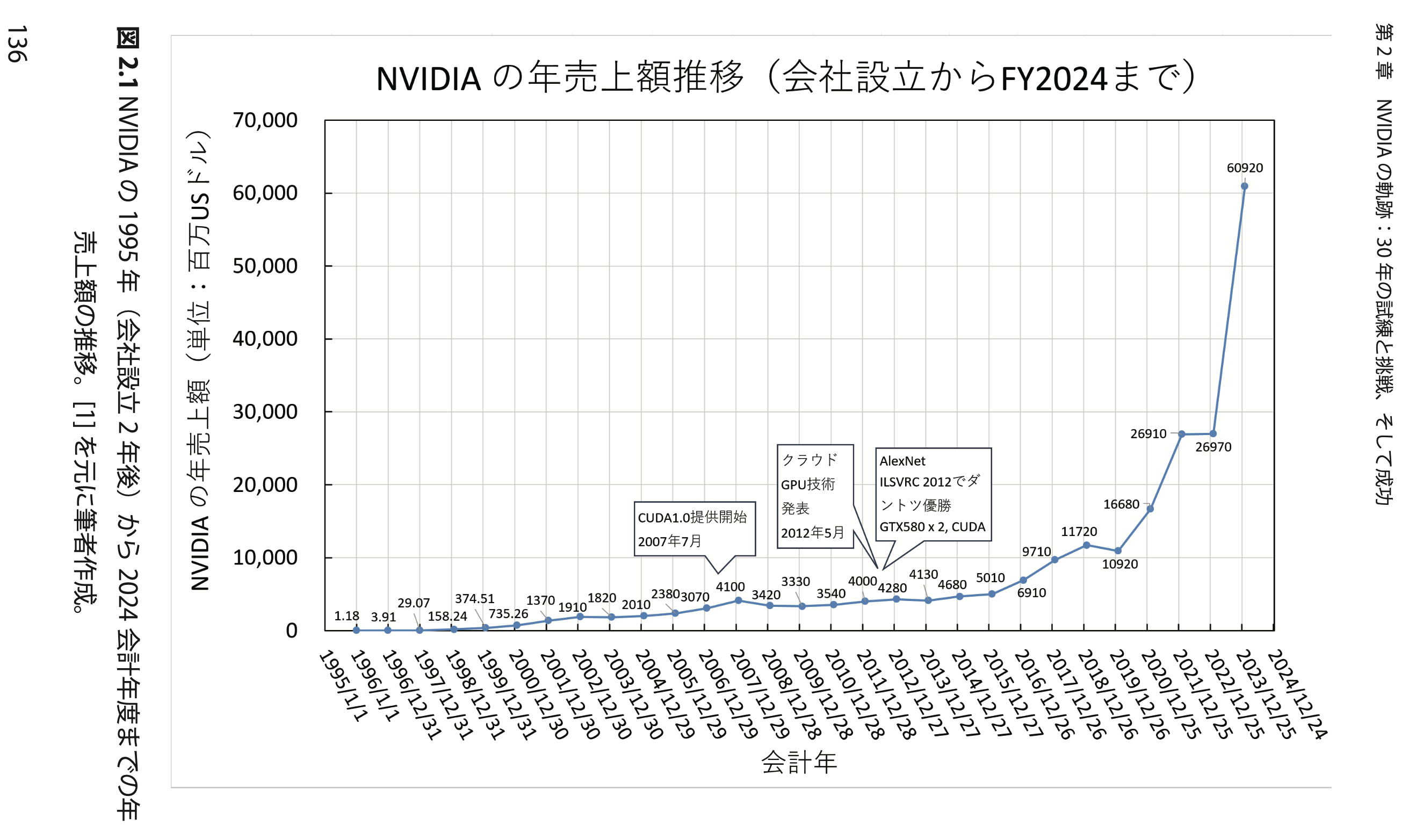
However, there are also movements among companies and data center operators to “escape from NVIDIA.” In the AI chip market, companies such as AMD and Intel, as well as many emerging companies, are trying to challenge NVIDIA with innovative technologies in order to challenge its overwhelming position. In response, NVIDIA has listed the names of the challenging emerging companies on its website and “declared war” against these challengers in order to maintain its leadership. It is expected that these chips will be available in 2025, and the AI chip market will enter a “warring states period.”
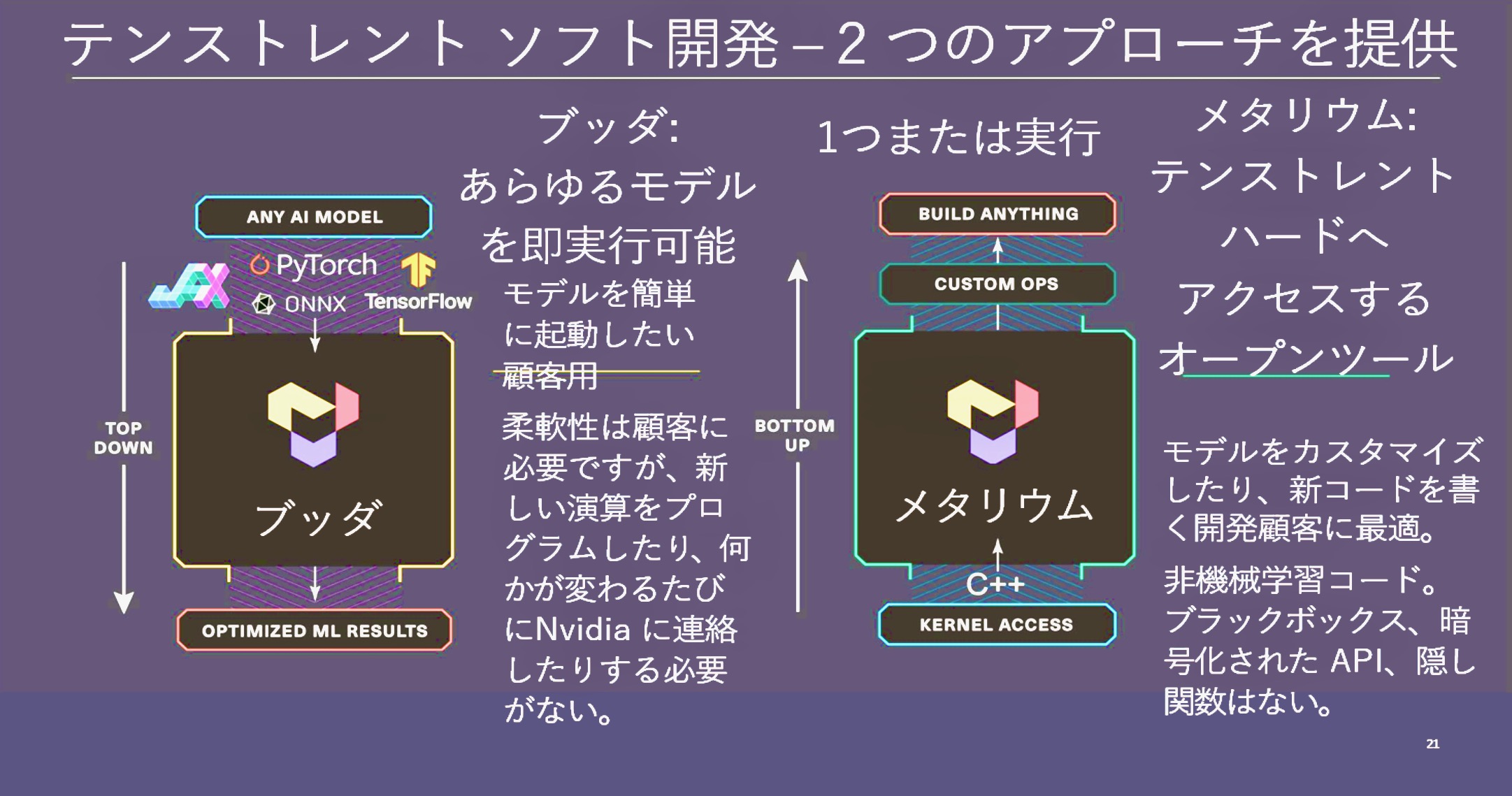
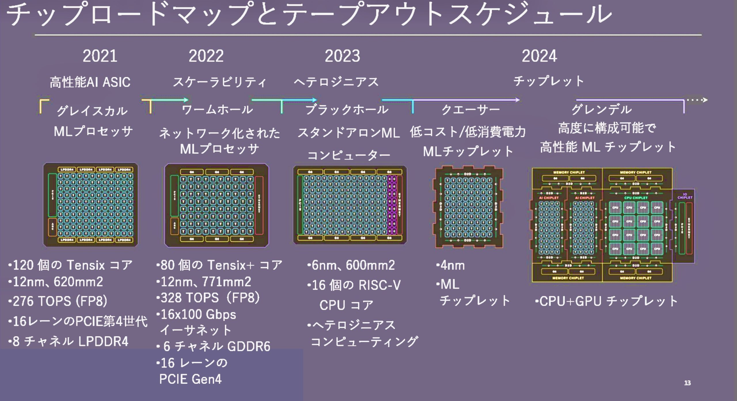
Figure. Tenstorrent AI chip roadmap challenging NVIDIA
● Chapter 4 “Arm’s new strategy: Improving performance, efficiency, and area with TSMC-optimized IP”
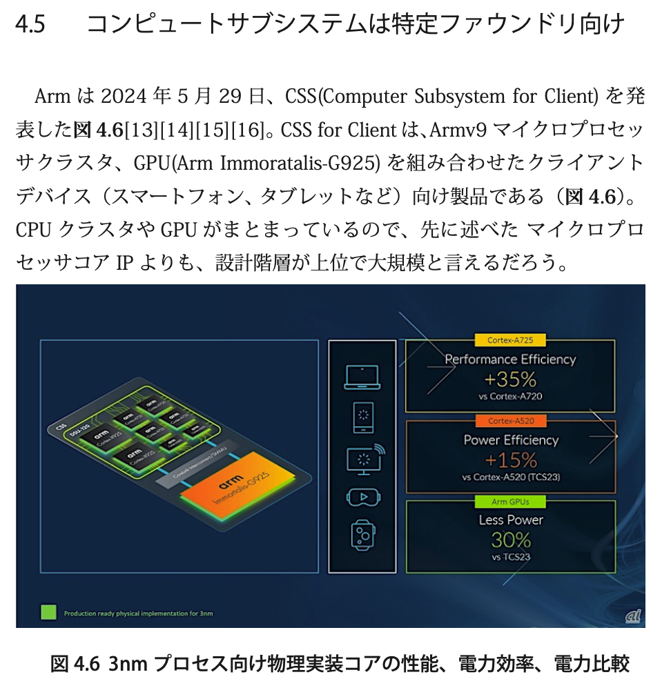
In recent years, Arm has launched a new strategy to improve the performance, efficiency, and area (PPA: Performance, Power, Area) of semiconductor chips by providing “semiconductor IP (Intellectual Property) optimized for manufacturing at TSMC”. This strategy is designed specifically to fit the most advanced processes (5nm, 3nm, etc.) at TSMC in Taiwan, and supports user companies in enabling competitive chip designs. As semiconductor technology advances, the development costs of each process node rise, requiring close optimization of the manufacturing process and IP. TSMC leads other foundries in advanced processes such as 5nm and 3nm, and providing optimized IP to match this is a major competitive advantage for Arm. Arm’s TSMC-optimized IP strategy is a strategy to meet current market needs.
● Chapter 5: TSMC’s 24 Years: Sales Trends and Technology Node Changes
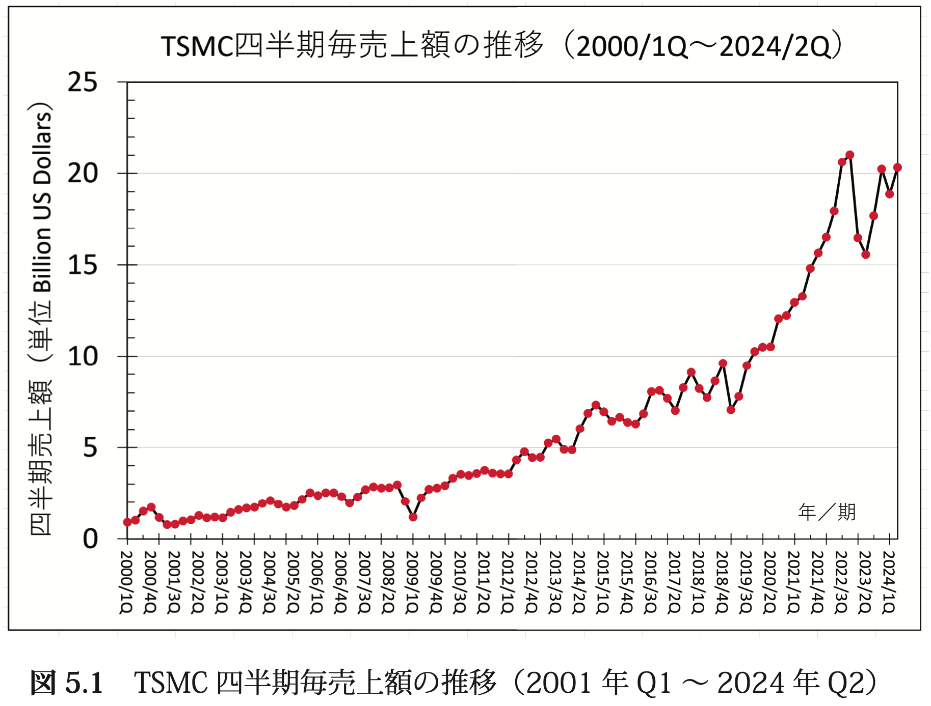
As of 2024, it can be said that the fabless semiconductor model has won over the integrated semiconductor model (IDM). Intel lost to TSMC at the 10nm process node, and TSMC took the lead in cutting-edge technology. Intel’s 10nm process node continued to be delayed, while TSMC commercialized 7nm and 5nm process technologies and established its dominance in the advanced semiconductor market. When Apple switched from purchasing chips from Intel to designing them in-house and outsourcing manufacturing to TSMC in 2020, Intel’s technological advantage was greatly shaken. This dramatic change greatly shook the balance of power between fabless semiconductor manufacturers (TSMC is responsible for manufacturing) and integrated semiconductor manufacturers (IDMs), and TSMC became the world’s business leader.
Patrick Paul Gelsinger, who served as Intel’s CEO until December 2024, promoted reforms aimed at entering the dedicated foundry business while maintaining the company’s vertically integrated semiconductor company, or IDM (Integrated Device Manufacturer) model. Intel has set a strategy called “IDM 2.0” and aims to balance the department that designs and manufactures its own products with the department that provides foundry services to external customers.
On the other hand, TSMC continues to grow rapidly as the focus of technology leadership shifts from mobile to AI data centers, with major companies such as NVIDIA as customers. In particular, the transition to the 2nm process is expected to bring about major changes in the semiconductor market, and TSMC’s role is expected to remain highly important in the future. As a result, technological innovation and changes in the competitive environment require continued attention.
● Chapter 6 RISC-V Development with DARPA Automated Design Flow and Google Support Shuttle
Since 2018, DARPA (Defense Advanced Research Projects Agency) has been developing “Open Road,” a set of open source tools for automating semiconductor design.
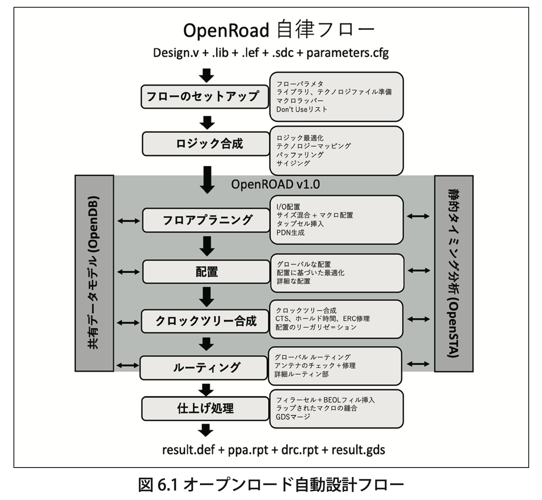
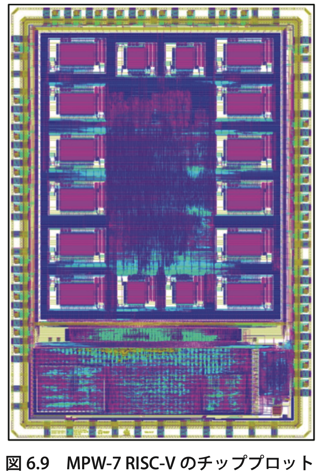
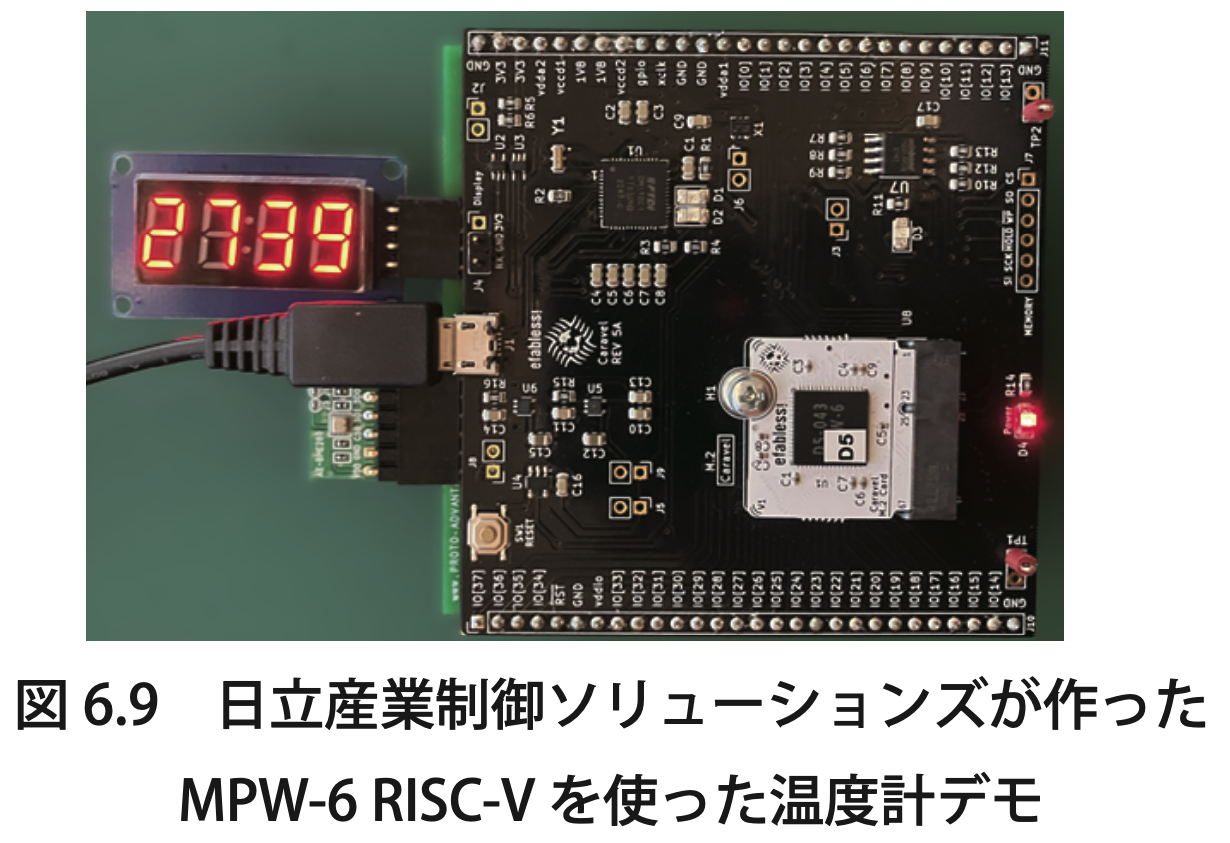
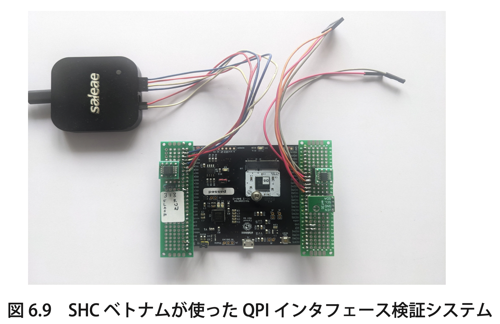
In 2022, we used the Google free shuttle and, as part of a NEDO-commissioned project, used the “Open Road” tools to tape out small SoC chips such as RISC-V and SH-2 three times. At the end of 2023, just when we had almost forgotten about it, three shuttle prototypes manufactured at the SkyWater fab arrived from eFabless. From March 2024, with the cooperation of the Japan Embedded Systems Technology Association (JASA), we were able to evaluate the first MPW-6 (RISC-V) prototype. It operated normally at 25 MHz (megahertz), and we experienced the usefulness of “Open Road” in reality. The reliability of the design flow was confirmed, and we are currently evaluating the external flash memory and PSRAM high-speed interface IP functions.
● Chapter 7 Andes Growing with RISC-V: The Future of Taiwan’s No. 1 IP Company
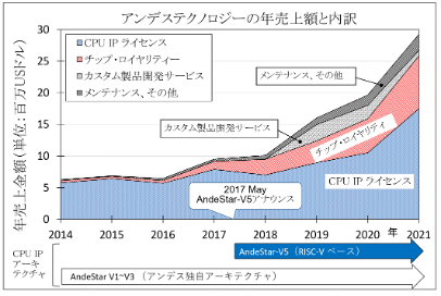
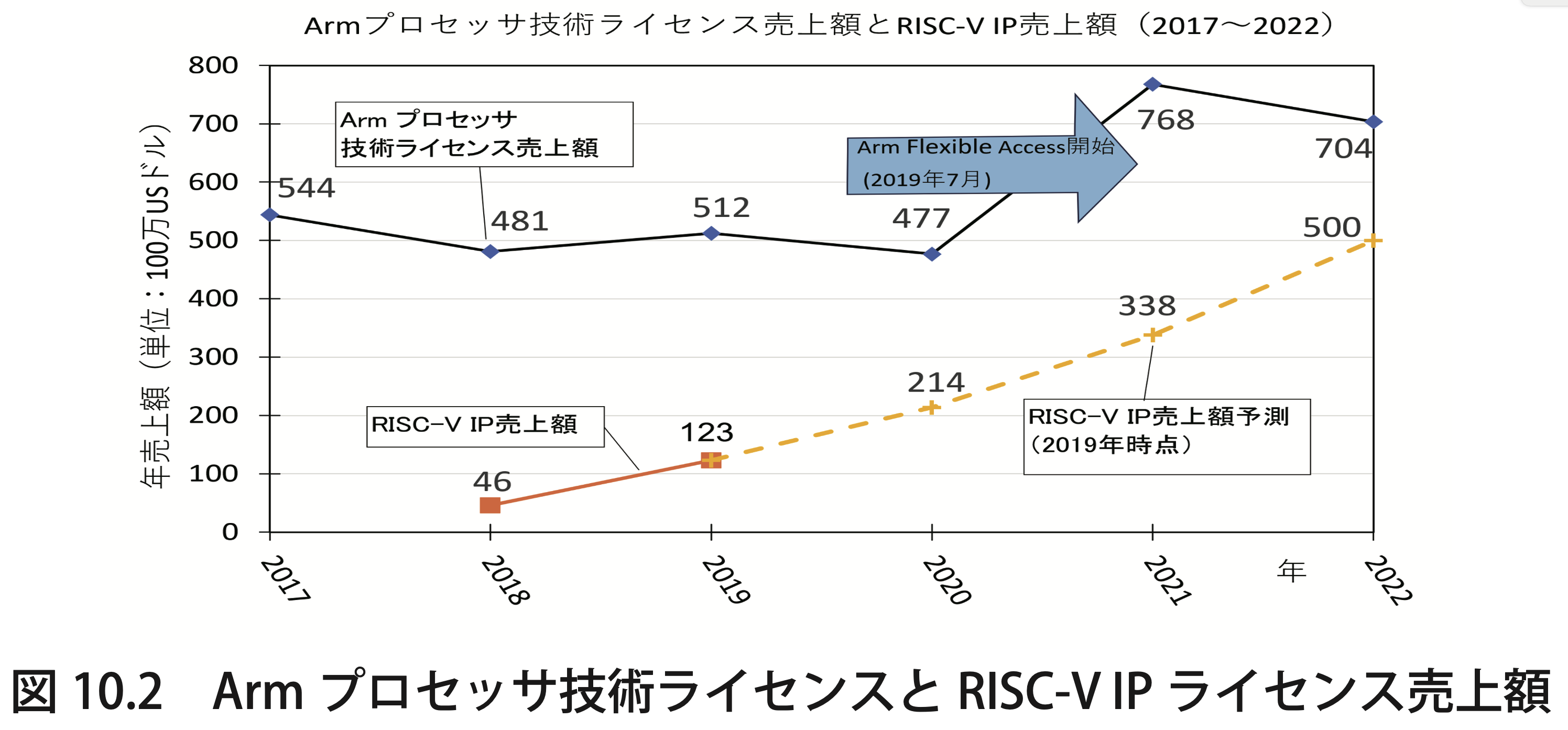
Andes Technology is a listed company that has been trading on the Taiwan Stock Exchange (TWSE) since December 2020 under the stock code “6533”. With an average annual growth rate of about 52% over the past few years, it is Taiwan’s No. 1 semiconductor IP provider that may catch up with and overtake Arm in the early 2030s. Arm’s licensing model, which defined the fabless semiconductor model since the 1980s, has long been the industry standard.
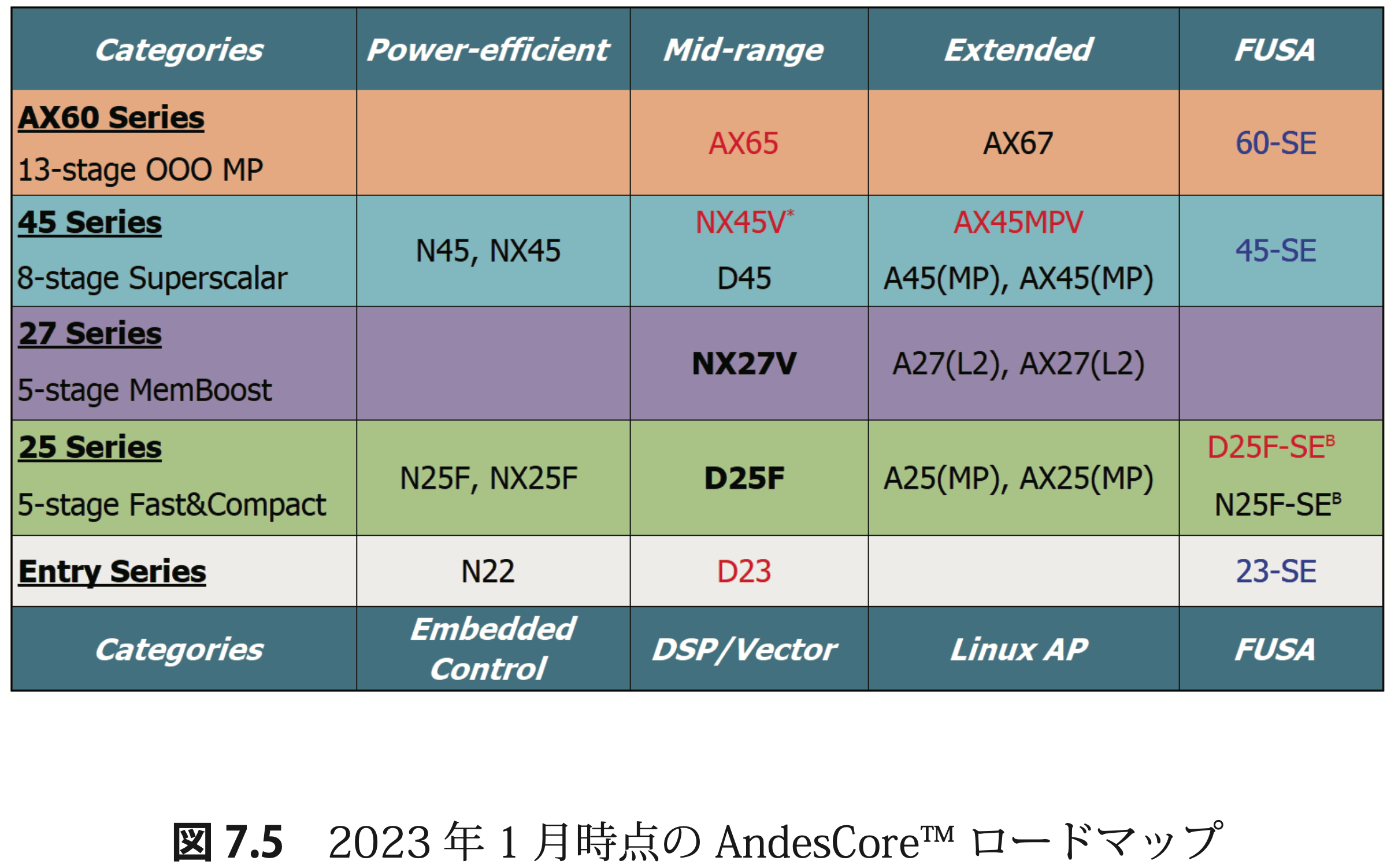
Since its establishment in 2005, Andes Technology has introduced a flexible licensing model to the market, challenging ARM’s low-end CPU IP with its low-end CPU IP, and major Japanese telecom equipment, mobile base station equipment, broadcasting equipment, semiconductor manufacturing equipment, and other companies have adopted Andes’ CPU IP one after another. Arm introduced its own flexible license as a countermeasure, but this had a significant impact on Arm’s revenue structure because it was less profitable than Arm’s traditional fixed license model. Andes Technology has adopted the open architecture RISC-V since 2016, which supports its current growth strategy.
● Chapter 8 Scalable RISC-V for DX provided by Tenstorrent
Tenstorrent is one of the companies that has declared that it will challenge NVIDIA. We transcribed and translated into Japanese the presentation that was given during the company’s visit to Japan on January 16, 2024. Tenstorrent plans to introduce a heterogeneous computing platform product called “Grandale” to the market and take on NVIDIA’s “Grace Hopper” head-on in 2025.
● Chapter 9 Easily debug RISC-V-based chips from microcontrollers to multi-core SoCs
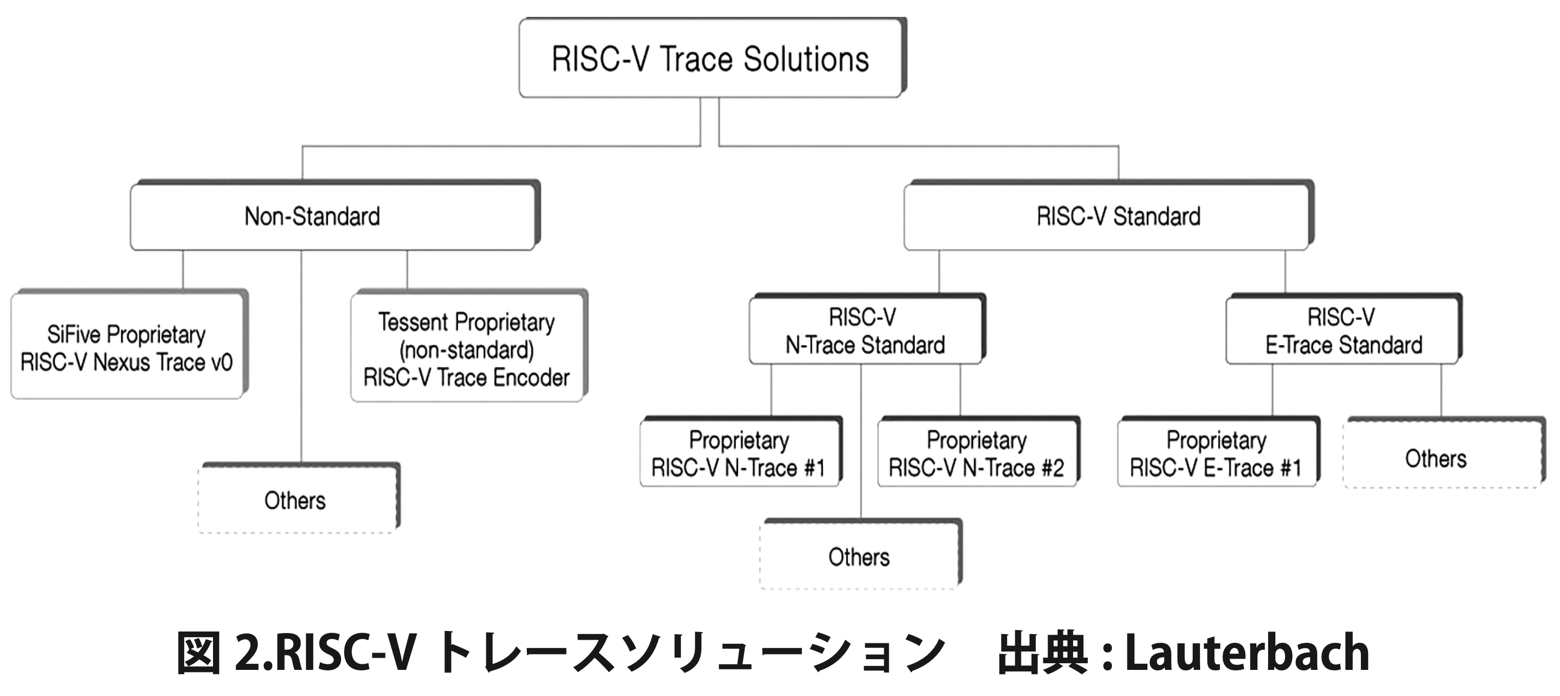
A high-end debugging emulator tool developed by Lauterbach that is used to improve the functional safety of software installed in automobiles, social infrastructure, medical equipment, etc. By preventing problems from being created during the design process, it improves the safety and reliability of the final product. Automotive, social infrastructure, and medical equipment applications require an advanced debugging environment to support functional safety.
● Chapter 10 RISC-V and the US-China conflict: Open source cooperation continues beyond the divide
RISC-V is an open industrial standard, and its unique feature is that companies and research institutes around the world, whether allied or non-allied, are developing processors and related technologies based on the same standard. Many countries, including Russia and China, are independently developing and using RISC-V.
In 2023, some US lawmakers considered export restrictions on RISC-V technology, but because RISC-V is an open standard and is not limited to a specific technology or implementation, restrictions were deemed difficult, and ultimately no restrictions were imposed. The basic design based on the common specifications of RISC-V also makes it compatible with technologies developed in both the United States and China. However, due to export restrictions and the influence of the US-China conflict, cooperation between the two countries in the development of application software and hardware has decreased, but cooperation on basic technology (mainline) specifications continues to this day.
[Commentary] Rapidus’ challenge to 2nm manufacturing is a symbolic effort for Japan’s semiconductor industry to revive. This book explains the key elements that will open up the 2nm era against the backdrop of competitors such as NVIDIA and AMD, and the efforts of Japan’s industrial sector. Against the backdrop of the AI era, it depicts from a multifaceted perspective how Japan is facing global competition in semiconductors and trying to establish technological leadership while collaborating and competing with NVIDIA and AMD. Japan’s 2nm semiconductor strategy, its challenges and future. We will introduce the challenges and solutions that Japanese companies, including Rapidus, face in semiconductor manufacturing using microfabrication technology.Challenge 1: Establishing technical capabilities
GAA (Gate-All-Around) transistors, back-side power distribution (BSPD), and yield rate
Challenge 2: Playing a part in the global semiconductor supply chain
Moving from vertical integration to horizontal division of labor
Challenge 3: Semiconductor human resource development and fundraising
Lack of human resources to support advanced manufacturing technology and long-term funding plans
Challenge 4: Global competition
How to compete with leading companies such as TSMC and Samsung. Challenge 5: Policies and fundraising mechanisms to support technological innovation
We will analyze the factors that will determine the success or failure of the AI semiconductor support policy announced by Prime Minister Ishiba.
Hardcover: 492 pages (147 x 209 mm)
Price: 2,000 yen (excluding tax)
Editor: Taho Haruyuki, Supervisor: Tanabe Izumi, Binding: Nakajima Takayuki
Release date: November 1, 2024, 1st edition, 1st printing
Sales locations: Major bookstores, online stores, and our own website (https://sohacoinc.square.site/)
For more information, please contact Nishimura Shoten Co., Ltd., a wholesaler specializing in natural science books. Publisher: Shunpei Kawasaki
Published by: Sohaco Publishing Co., Ltd.
Recommended by: RISC-V Association
7-18-13, Ginza, Chuo-ku, Tokyo
Tel: 03-5565-0556, Main: 03-3833-3717
Email: sohaco@swhwc.com
Book code: ISBN 978-4-91109-09-2
Category code: C0034
Price: 2000 yen + tax
Published by: Sohaco Publishing Co., Ltd.
Technology B2-53 Hardware Development
Computer Architecture B8-02
Deep Learning
[Table of Contents]
• Preface vii
1. Japan’s Semiconductor Strategy and RAPIDUS: Integrating Diplomacy, Security, and Economic Policies 1
1.1 Why 2nm Do we need fabs? 1
1.1.1 Competitive reset effect of new technology introduction 1
1.1.2 Introduction of GAA transistor technology 2
1.1.3 EUV (extreme ultraviolet) lithography technology 3
1.1.4 Backside power distribution (BSPD) technology 3
1.1.5 New partnerships and access to manufacturing facilities 3
1.1.6 Common learning curve for established companies and new entrants 4
1.1.7 Riding the timing of a paradigm shift 4
1.2 65-year history of MOSFET (metal-oxide-semiconductor) 4
1.2.1 Japanese companies withdraw from the development race with planar MOSFET 6
1.2.2 FinFET deployment globally 8
1.2.3 FinFET developed from the idea of Japanese engineers 9
1.2.4 Japanese engineers who followed FinFET (2014) 10
1.2.5 Transition to GAA (Gate-All-Around) at 2nm (2024) 11
1.2.6 Is GAA an evolution rather than a revolution from FinFET? 12
1.3 “Next-generation technologies” associated with the 2nm process 15
1.3.1 Improve performance and area with backside power delivery (BSPD) 16
1.3.2 Through-silicon via (TSV) 17
1.3.3 Intel has already completed backside power delivery at 2nm 18
1.3.4 Intel also discloses backside power delivery wafer manufacturing method 19
1.3.5 Intel predicts that backside power delivery will not increase costs 20
1.3.6 Increased use of EUV for 2nm frontside power delivery (FSPD) 20
1.3.7 Intel says backside power delivery will not degrade yields 21
1.3.8 Through-silicon vertical electrical interconnects are necessary for 3D stacking 21
1.3.9 Interposers are essential for 2.5D stacking 22
1.3.10 Intel and AMD develop their own chiplets 22
1.3.11 Intel’s proprietary chiplet technology “Foveros” 23
1.3.12 AMD also develops its own chiplet technology 25
1.3.13 Chiplet technology at NVIDIA 28
1.3.14 Chiplet interoperability and standardization 30
1.3.15 UCIe (Universal Chiplet Interconnect Express) 31
1.3.16 AIB: Advanced Interface Bus (2018) 32
1.3.17 10 companies dominating Die-to-Die (D2D) standards 33
1.3.18 The business of selling chiplets 35
1.3.19 Alpha Wave Semi’s chiplet business 36
1.3.20 3D and 2.5D stacking technology and backside power supply 36
1.3.21 Extreme ultraviolet lithography (EUV) at advanced nodes 37
1.4 TSMC’s status of 2nm and beyond 40
1.4.1 TSMC’s EUV adoption status 40
1.4.2 TSMC’s roadmap for 2nm and beyond: 41
1.5 Samsung 2nm roadmap 43
1.6 Intel’s 2nm roadmap 45
1.7 Rapidus’ 2nm fab 47
1.7.1 The significance of Japan having a next-generation semiconductor fab 47
1.7.2 Rapidus’ 2nm schedule 48
1.7.3 Is the Rapidus 2nm schedule too late? 48
1.8 Eight major industries that make up the semiconductor supply chain 50
1.8.1 EDA (Electronic Design Automation) companies? 50
1.8.2 IP (Intellectual Property) providers 50
1.8.3 Fabless semiconductor companies 51
1.8.4 Semiconductor manufacturing companies (foundries) 51
1.8.5 IDM (Integrated Device Manufacturers) 51
1.8.6 OSAT (Outsourced Semiconductor Assembly and Test) 52
1.8.7 Semiconductor material suppliers companies 53
1.8.8 Semiconductor manufacturing equipment manufacturers 53
1.9 Overview of Japan’s semiconductor strategy 54
1.9.1 Strengthening the semiconductor manufacturing base 54
1.9.2 Semiconductor-related companies entering the market and creating jobs to stimulate the local economy: 54
1.9.3 Quantitative targets for semiconductor revival (achieving 15 trillion yen in sales in 2030) 55
1.9.4 Supplementary budget for semiconductors 56
1.9.5 Enforcement of new law and huge investment: measures to strengthen domestic semiconductor fabs 57
1.9.6 Establishment of new tax system to promote production in the domestic semiconductor industry 60
1.10 Global semiconductor competition 61
1.10.1 Initiatives of major countries 61
1.10.2 Securing next-generation semiconductors 62
1.10.3 Initiatives for manufacturing next-generation logic and memory semiconductors 62
1.10.4 Establishment of cutting-edge semiconductor manufacturing ecosystem 63
1.10.5 Lapidus Co., Ltd. 66
1.10.6 Additional support for Lapidus 67
1.10.7 Lapidus’ future business phase and support 69
1.10.8 Beyond 2nm Semiconductor technology for the next generation 70
1.10.9 Began investment support for cutting-edge semiconductors ahead of the rest of the world 72
1.11 Developing use cases for next-generation semiconductors 73
1.11.1 Hierarchical structure of services in AI and computing 73
1.11.2 Memory and storage strategies 74
1.11.3 Direction of memory for AI calculations 75
1.11.4 Recent efforts toward realizing next-generation semiconductors 77
1.11.5 Rapidus West Coast base (Rapidus Design Solutions) 78
1.11.6 Collaboration with Tenstorrent and Esperanto 79
1.11.7 Why are chiplets needed for next-generation semiconductors? 80
1.11.8 Importance of advanced packaging strategy and efforts 82
1.11.9 Development of advanced packaging technology for advanced semiconductor back-end processing 83
1.12 Leading-edge Semiconductor Technology Center (LSTC) 85
1.12.1 Organization of the Leading Semiconductor Technology Center (LSTC) 85
1.12.2 LSTC research and development projects 86
1.13 Diplomatic benefits of advanced semiconductors 88
1.13.1 Legacy semiconductor industrial support and economic security 88
1.13.2 Survey on legacy semiconductors in the United States 88
1.13.3 Ensuring security in semiconductor-related industries 89
1.13.4 Risks of technology and data leakage and countermeasures 90
1.13.5 International semiconductor cooperation 91
1.13.6 Japan-US summit and Japan-US-Philippines summit 93
1.13.7 The 3rd Japan-US Commercial and Industrial Partners (JUCIP) Meeting 94
1.13.8 Japan-EU semiconductor cooperation 95 1.13.9 Japan-UK semiconductor cooperation 96
1.13.10 Semiconductor cooperation between Japan and the Netherlands 97
1.13.11 Overview of R&D support systems in the US and EU 98
1.14 Financial sustainability of Japan’s semiconductor strategy 100
1.14.1 Contents of the Financial System Subcommittee (held on April 9, 2024) 100
1.14.2 Scale of semiconductor support measures in each country (reflecting tax systems and the latest situation) 101
1.15 Semiconductor strategies in countries around the world 102
1.15.1 Semiconductor support projects in the US 102
1.15.2 TSMC overseas investment and government support: A comparison of countries 104
1.16 Power demand and semiconductors 106
1.16.1 Power demand for data centers 106
1.16.2 Attracting AI data centers (DC) and energy measures 107
1.16.3 AI data center initiatives by general electricity transmission and distribution companies 110
1.16.4 GX Green Transformation Executive Committee 111
1.16.5 Energy supply to support AI and data centers 112
1.16.6 AI data centers and advanced computing resources 113
1.16.7 Optimization of AI computing infrastructure and power consumption management 115
1.17 Semiconductor human resource development 118
1.17.1 Establishment of advanced semiconductor development and human resource development center 118
1.17.2 Strengthening R&D and human resource development through LSTC activities 119
1.17.3 Collaboration with overseas institutions and human resource development 120
1.17.4 Efforts to develop semiconductor human resources 121
1.17.5 Efforts to develop semiconductor human resources in the Tohoku region 122
1.17.6 The importance of highly skilled human resource development and specific efforts 122
1.17.7 Strengthening the supply chain of semiconductor materials 123
1.17.8 LSTC Human Resource Development Working Group (WG) 124
1.17.9 Regional consortium to promote semiconductor human resource development 126
1.18 Economic ripple effects on local communities 127
1.18.1 Economic ripple effects on Kumamoto Prefecture 127
1.18.2 Advancement and investment of semiconductor-related companies in Kumamoto Prefecture 128
1.18.3 Prime Minister Kishida, TSMC, and local companies roundtable 129
1.18.4 Support for strengthening the semiconductor supply chain with the Economic Security Fund 130
1.19 Sources 134
2. NVIDIA’s history: 30 years of trials, challenges, and successes 135
2.1 Trends in NVIDIA sales 135
2.2 Market share of desktop PC GPU cards by company 139
2.3 NVIDIA AI semiconductors for data centers 140
2.4 References 141
2.5 Collaboration between NVIDIA and Taiwanese semiconductor manufacturing: Success built through cooperation 143
2.5.1 1960s Challenges and transformation starting from back-end processing 143
2.5.2 1970s Introduction of front-end technology and application-oriented management strategy 144
2.5.3 1980s Pure-play foundries that changed the semiconductor industry 148
2.5.4 Growth of TSMC 151
2.5.5 Taiwan’s semiconductor manufacturing industry and NVIDIA 153
2.5.6 References 154
3. Graphics and AI revolution: Jensen Huang and NVIDIA’s challenge 155
3.1 NVIDIA and Jensen Huang 155
3.2 NVIDIA’s founding 156
3.2.1 NVIDIA’s founding (1993) 156
3.2.2 Jensen Huang (Huáng Rénxūn) 156
3.2.3 Co-founders 159
3.3 The early days of NVIDIA (1993) 168
3.3.1 The origin of the NVIDIA name 168
3.3.2 3D graphics technology at the time of NVIDIA’s founding 171
3.4 First product: NV1 175
3.4.1 Manufacturing partnership with STMicro (1995) 175
3.4.2 Microsoft DirectX (1995) 180
3.4.3 NV2 for Sega (1995) 180
3.4.4 Quiet pivot (1996) 181
3.4.5 Cut 50% of staff 182
3.4.6 Closed cafeteria but continued nightly pizza orders 186
3.4.7 NV1 returns piled up to create a monument 187
3.4.8 NVIDIA returns to stealth and starts anew 189
3.4.9 Sega’s internal next-generation console development contest (1996) 191
3.4.10 11 people from Sega of America transfer to Hitachi (1996) 194
3.4.11 What happened to 3dFx (1996) 194
3.4.12 The aftermath of the Black Belt vs. Katana battle (1996) 195
3.4.13 The Bubble Economy (1992) and the Arm’s Length Principle (1994) 196
3.4.14 A $7 million MOU written on a napkin (1996) 197
3.4.15 Amicable termination of the NV2 development contract with Sega (1997) 199
3.4.16 Dreamcast goes to Imagination (1997) 200
3.4.17 Hitachi Semiconductor faces financial difficulties due to sudden changes in the DRAM market (1996) 201
3.5 From 3D accelerators to GPUs (NV3-NV20) 201
3.5.1 Microsoft promotes DirectX (September 1995) 201
3.5.2 TSMC from NVIDIA’s perspective (1996) 205
3.5.3 NV3: RIVA 128 captures 10-15% market share (1997) 207
3.5.4 NV10: GeForce 256 (1999) named GPU 209
3.5.5 GPU driver source not disclosed (1999) 213
3.5.6 Programmable GPU: NV20: GeForce 3 (2001) 214
3.6 OS development at NVIDIA 217
3.6.1 Size of NVIDIA’s OS development team 218
3.6.2 Why NVIDIA is so enthusiastic about OS development 218
3.6.3 Are 99% of blue screens caused by NVIDIA drivers? 221
3.6.4 Graphics benchmarks in 2000 223
3.7 NVIDIA financials 223
3.7.1 Jensen’s shareholding at NVIDIA’s IPO 224
3.7.2 Debt-free management 224 3.7.3 NVIDIA’s largest shareholders 225
3.8 2000s: Diversification and market dominance 226
3.8.1 Expansion into new markets: data centers, automotive, etc. 226
3.8.2 Major new product generation launches and technology advances 231
3.9 Gaining technological advantage through acquisitions 234
3.9.1 Acquisition of 3dfx Interactive (2000) 234
3.9.2 Acquisition of MediaQ and the Tegra series (2003) 235
3.10 Strategic partnerships 237
3.10.1 Sony Playstation 3 (2000s) 237
3.10.2 Microsoft Xbox 360 (2000s) 238
3.10.3 IBM HPC High Performance Computing (2000s) 238
3.10.4 Audi Google Earth Navigation (2000s) 238
3.10.5 NVIDIA orders 20 SH7786 evaluation boards from Hitachi 240
3.10.6 Tesla Motors (2000s) 243
3.11 Steady business expansion behind the scenes of the AI revolution 243
3.11.1 The advent of AI deep learning 243
3.11.2 NVIDIA GPUs become essential for AI research and development 245
3.11.3 NVIDIA GPUs CUDA democratizes AI development 246
3.11.4 Impact on industry 247
3.12 CUDA platform 247
3.12.1 Popularization of large-scale parallel computing with CUDA 248
3.12.2 CUDA parallel computing model 249
3.12.3 Support for processing order and data dependency 249
3.12.4 How parallel processing works in CUDA 249
3.12.5 Memory hierarchy and data transfer 250
3.12.6 CUDA libraries (parallel computing software stack): 251
3.12.7 CUDA’s contribution to computer science 252
3.12.8 CUDA gives wings to AI researchers 253
3.12.9 CUDA transforms industry: from genomics to robotics 254
3.13 The beginning of CUDA: Cg, the C language for graphics 254
3.13.1 What is a programmable shader? 255
3.13.2 The history of programmable shaders 255
3.13.3 NVIDIA’s own shader compiler development 256
3.13.4 Market response to NVIDIA’s shader compiler CG 257
3.13.5 The origin of the word “CUDA” 259
3.13.6 The quantum leap from CG to “CUDA” 260
3.13.7 GPU development tool “CUDA Toolkit” 261
3.13.8 CUDA debugging tool NVIDIA Nsight 262
3.13.9 GPU documentation and support 262
3.14 Is software a “service that only causes loss” for chip companies? 263
3.14.1 Early Jensen’s thoughts on software 263
3.14.2 Jensen’s critique of the “SH franchise” 264
3.14.3 What NVIDIA learned from “NV1” at the time 265
3.14.4 Initial opposition to expanding Cg compiler development staff (2003) 266
3.14.5 Engineers’ feelings after the IPO (2003) 267
3.14.6 Linus, Stallman, and open source 267
3.14.7 Recruiting Windows OS developers from NVIDIA 269
3.14.8 Excellent engineers from NVIDIA 270
3.14.9 A young Cg compiler engineer fighting alone (2002) 271
3.14.10 Conditions for being called a general-purpose GPU 273
3.14.11 CUDA highlights ease of GPU programming 273
3.14.12 References 274
3.15 Mobilizing researchers to promote NVIDIA 274
3.15.1 Google TensorFlow optimized for NVIDIA 274
3.15.2 Google Cloud integration 275
3.15.3 GPU services provided by Amazon Web Services (AWS) 275
3.15.4 Accelerating AI research with Amazon Machine Images (AMI) 275
3.15.5 Microsoft: Azure Machine Learning integration 275
3.15.6 AI research collaboration with universities 276
3.16 NVIDIA’s cutting-edge AI chip architecture 277
3.16.1 NVIDIA GPU architecture direction 277
3.16.2 NVIDIA History of GPU architecture 278
3.16.3 Linking GPU architecture with CUDA 279
3.17 Tensor Core 280
3.17.1 Acceleration of matrix operations 281
3.17.2 Implementation of matrix multiplication (Fused Multiply-Add, FMA) 282
3.17.3 Support for multi-precision operations 282
3.17.4 Linking with the Transformer Engine 283
3.17.5 Application areas where the Tensor Core is useful 283
3.18 Hopper architecture 284
3.18.1 Features of the Hopper architecture 284
3.19 Transformer Engine 285
3.19.1 Background of the Transformer architecture 285
3.19.2 Details of the Transformer Engine 285
3.19.3 Applications of the Transformer Engine 286
3.20 Dynamic Programming (DP) 287
3.21 Simultaneous execution of multiple tasks with MIG (Multi-Instance GPU) 287
3.22 NVLink 4.0 speeds up GPU-GPU-CPU transfers 288
3.23 HBM3 memory (High Bandwidth Memory 3) 288
3.24 AI chips challenging NVIDIA 290
3.24.1 “The Warring States period of AI will begin in 2025” 290
3.24.2 Major IT companies enter the race with their own AI chips 291
3.24.3 AMD pursues CUDA with RDNA and ROCm 291
3.24.4 Intel competes by acquiring Ponte Vecchio, Gaudi, and Mobileye 295
3.24.5 Google replaces NV with cloud AI using TPU 300
3.24.6 Tesla develops self-driving AI chip Full Self-Driving in-house 300
3.24.7 Amazon develops AI chips Trainium and Inferencia in-house 301
3.24.8 Qualcomm challenges with mobile and in-vehicle AI chips 301
3.24.9 Apple challenges NVIDIA with M-series built-in GPU 302
3.24.10 Tenstorrent “Grayskull” and “Wormhole” from Graphcore 302
3.24.11 Graphcore’s Intelligence Processing Unit 303
3.24.12 Cerebras Systems’ Wafer Scale Engine 303
3.24.13 SambaNova’s Reconfigurable Dataflow Unit 304
3.24.14 Mythic AI’s Analog AI Inference Chip 305
3.24.15 Groc’s Tensor Streaming Processor 305
3.24.16 NVIDIA Challengers Roundup 306
3.25 NVIDIA Innovations Start Transforming Industries 307
3.25.1 Healthcare and Life Sciences 307
3.25.2 Autonomous Vehicles and Transportation 308
3.25.3 Manufacturing and Robotics 309
3.25.4 Finance and banking 309
3.25.5 Financial risk management and compliance applications 310
3.25.6 Media and entertainment 310
3.26 References 311
3.27 Conclusion 311
3.28 Musings 311
4. Arm’s new strategy: Improving performance, efficiency, and area with TSMC-optimized IP 315
4.1 Trends in Arm revenue and shipments 315
4.2 Expansion of Flexible Access 315
4.3 Evolution of embedded Arm architecture and IP 317
4.4 Examples of embedded chip products 320
4.5 Compute subsystems are for specific foundries 320
4.6 References 321
5. TSMC’s 24 years: Trends in revenue and technology nodes 323
5.1 TSMC sales trends 323
5.2 Profit and profit margin 326
5.3 References 327
6. DARPA automated design flow for RISC-V prototype on Google-funded shuttle 329
6.1 Realizing MARMOT RISC-V with 1MB+ memory 330
6.2 Good fortune comes with Google free shuttle 331
6.3 Efabless Caravel Harness 332
6.4 Linux-based IoT edge and RTOS-based IoT edge 333
6.5 Open Road work log (2022) 333
6.6 Software verification of Efabless prototype chip (2024) 335
6.7 MPW-6 demo (August 1, 2024, November 20th) 338
6.8 “JASA1 Chip Evaluation Board” for distribution to members (Planning stage) 339
6.8.1 Cost image of “JASA1 Chip Evaluation Board” 340
6.8.2 Initialization of Dual and Quad connection with QPI flash (Completed) 341
6.8.3 Actual evaluation of QPI flash direct execution performance (In progress) 342
6.8.4 Release of Chisel source code (In progress) 342
6.8.5 Direct execution from QPI flash via cache 344
6.8.6 MPW-7 Marmot allows high-speed operation of 50MHz 344
6.8.7 Chisel verification with logic simulation and FPGA 344
6.8.8 MPW-7 Marmot’s PSRAM direct execution function to JASA1 345
6.9 Chisel study session 346
6.9.1 “Starting Digital Circuit Design with Chisel” 346
6.9.2 Verifying Chisel’s operation on Arty A7 FPGA 347
6.10 Future Plans 347
6.11 MPW-8 releases its own SH-2 348
6.12 Impressions 349
6.13 Conclusion 349
6.14 Acknowledgements 349
7. Andes Growing with RISC-V: The Future of Taiwan’s No. 1 IP Company 351
7.1 Andes Technology with a 30% share of RISC-V 351
7.2 CPU IP lineup and strategy for 2030 354
7.3 Vision for 2030 361
7.4 References 363
8. DX provided by Tenstorrent Scalable RISC-V for 365
9. From simple microcontrollers to complex multi-core SoCs
– Debugging RISC-V-based chips made easy 391
10. RISC-V and the US-China conflict: Open source cooperation continues beyond the divide 401
10.1 Introduction 401
10.2 Origin and basic characteristics of RISC-V 401
10.2.1 What is an instruction set architecture, ISA? 402
10.2.2 Strategic privileges for companies that control the “instruction set” 404
10.2.3 Why RISC-V emerged 404
10.2.4 Why Google is supporting RISC-V on a large scale 405
10.2.5 40-year history of the “RISC instruction set” at the University of California, Berkeley 406
10.2.6 Differences between RISC-V’s business model and Arm’s 408
10.2.7 IP revenue and number of design starts surpass Arm (2023) 409
10.2.8 Arm leads RISC-V in fundraising through IPO 410
10.2.9 Arm withdraws request for Apple license fee increase 411
10.2.10 Performance comparison of cutting-edge RISC-V and cutting-edge Arm 412
10.2.11 Google and Qualcomm team up to complete Android for RISC-V, China also utilizes this 413
10.2.12 Bosch, Qualcomm, and Infineon’s in-vehicle RISC-V IP 415
10.3 More than 300 companies in China use RISC-V to develop products 416
10.3.1 T-Head (Pingtouge) RISC-V “Xuantie” 417
10.3.2 Alibaba “Xuantie” RISC-V system 418
10.3.3 HiSilicon RISC-V “Hi3861” 418
10.3.4 Huawei Hi3861 RISC-V ecosystem 419
10.3.5 StarFive’s RISC-V JH7110 SoC 421
10.3.6 China’s Terapines provides software-hardware co-design environment 422
10.3.7 Chinese Academy of Sciences “XiangShan” open RISC-V 423
10.4 Superchip embargo to China and RISC-V 424
10.4.1 US export restrictions on digital semiconductor technology to China 424
10.4.2 Response to Japanese government export restrictions 424
10.4.3 China and Taiwan hold talks at the 2023 European RISC-V Summit 426
10.4.4 US lawmakers request RISC-V export restrictions from Biden administration 426
10.4.5 Export restrictions on open industrial standards are difficult 427
10.4.6 Possibility of export restrictions on RISC-V cannot be denied 428
10.5 Japan’s semiconductor policy regarding RISC-V 429
10.5.1 RISC-V subsidy program led by METI 2018-2023 429
10.5.2 Confirmation of Japan-US economic security and technical cooperation at APEC2023 429
10.5.3 Japan-US cooperation on small nuclear reactors (SMR) announced immediately after APEC 2023 430
10.6 The creation of Rapidus as an integrated policy of the Japanese government 431
10.6.1 Integrating foreign policy, security policy, and economic policy 432
10.6.2 Strategic partnership between Rapidus and Tenstorrent 433
10.6.3 Expectations of the Japanese and US governments for Rapidus 434
10.6.4 Development of civilian and military dual-use manufacturing technology 435
10.6.5 NVIDIA manufactures military and civilian dual-use AI chips 436
10.6.6 Partnership between Rapidus and RISC-V CPU and AI chip companies 437
10.6.7 Partnership between Rapidus and Arm user semiconductor manufacturers 438
10.7 RISC-V’s footprint in the semiconductor industry 439
10.7.1 Applying open source philosophy to hardware design 439
10.7.2 The importance of open architecture in generative AI 440
10.7.3 Qualitative changes in semiconductor talent required by the evolution of electronic technology 440
10.7.4 Democratization of hardware design 441
10.7.5 RISE: Software support strategy for new architectures 442
10.7.6 The US and China compete for hegemony over RISC-V technology 442
10.7.7 Global cooperation through the Big Umbrella philosophy 443
10.7.8 References 446
• About the editors and authors 448
• Afterword 451

