Japan Semiconductor Strategy 2024+1/2: AI Chip Enterprise Challenge NVIDIA
– Rapidus’s challenge in 2nm semiconductor manufacturing
– The origins of NVIDIA’s AI semiconductor technology
– NVIDIA, Rapidus, and the roadmap to future semiconductors
– Painting the future of AI and semiconductors: Using NVIDIA as an example, we explore the 21st century innovation process brought about by technology and co-creation.
– For investors and policymakers: Includes extensive information on semiconductor-related stocks and government support measures.
– A reference for career development: A path to becoming an engineer in the semiconductor industry.
– NVIDIA’s unique evolution of AI chips and CUDA platform over the past 20 years.
– The secret behind the leadership and management philosophy of NVIDIA’s Jensen, a leader in the semiconductor industry.
– New AI market trends and innovative AI technologies that AMD and 15 startups are taking on.
– The potential for international cooperation and technological innovation centered on NVIDIA and Rapidus.
– Responding to the geopolitical risks brought about by the US-China conflict.
Challenge 1: Establishing technical capabilities
GAA (Gate-All-Around) transistors, backside power distribution (BSPD), and yield rate
Challenge 2: Playing a part in the global semiconductor supply chain
Moving from a vertically integrated model to a horizontal division of labor
Challenge 3: Semiconductor human resource development and fundraising
Lack of human resources to support advanced manufacturing technology and long-term funding plans
Challenge 4: Global competition
How to compete with leading companies such as TSMC and Samsung.
Topic 5: Policies and fundraising mechanisms to support technological innovation
Analyze the factors that will determine the success or failure of the AI semiconductor support policy announced by Prime Minister Ishiba.
Hardcover: 492 pages (147 x 209 mm)
Price: 2,000 yen (excluding tax)
Editor: Tago Haruyuki, Supervisor: Tanabe Izumi, Artwork: Nakajima Yoshiyuki
Release date: November 1, 2024, 1st edition, 1st printing
Sales locations: Major bookstores, online stores, and our own website (https://sohacoinc.square.site/)
For more information, please contact Nishimura Shoten Co., Ltd., a wholesaler specializing in natural science books. Publisher: Shunpei Kawasaki
Published by: Sohaco Publishing Co., Ltd.
Recommended by: RISC-V Association
7-18-13-502 Ginza, Chuo-ku, Tokyo
Tel: 03-5565-0556, Main: 03-3833-3717
Email: sohaco@swhwc.com
Book code: ISBN 978-4-91109-09-2
Category code: C0034
Price: 2000 yen + tax
Published by: Sohaco Publishing Co., Ltd.
Technology B2-53 Hardware Development
Computer Architecture B8-02
Deep Learning
• Preface vii
1. Japan’s semiconductor strategy and RAPIDUS: Integrating diplomacy, security, and economic policies 1
1.1 Why do we need a 2nm fab? 1
1.1.1 The competitive reset effect of new technology introduction 1
1.1.2 Introduction of GAA transistor technology 2
1.1.3 EUV (extreme ultraviolet) lithography technology 3
1.1.4 Backside power distribution (BSPD) technology 3
1.1.5 New partnerships and access to manufacturing facilities 3
1.1.6 Common learning curve for established companies and new entrants 4
1.1.7 Riding the timing of a paradigm shift 4
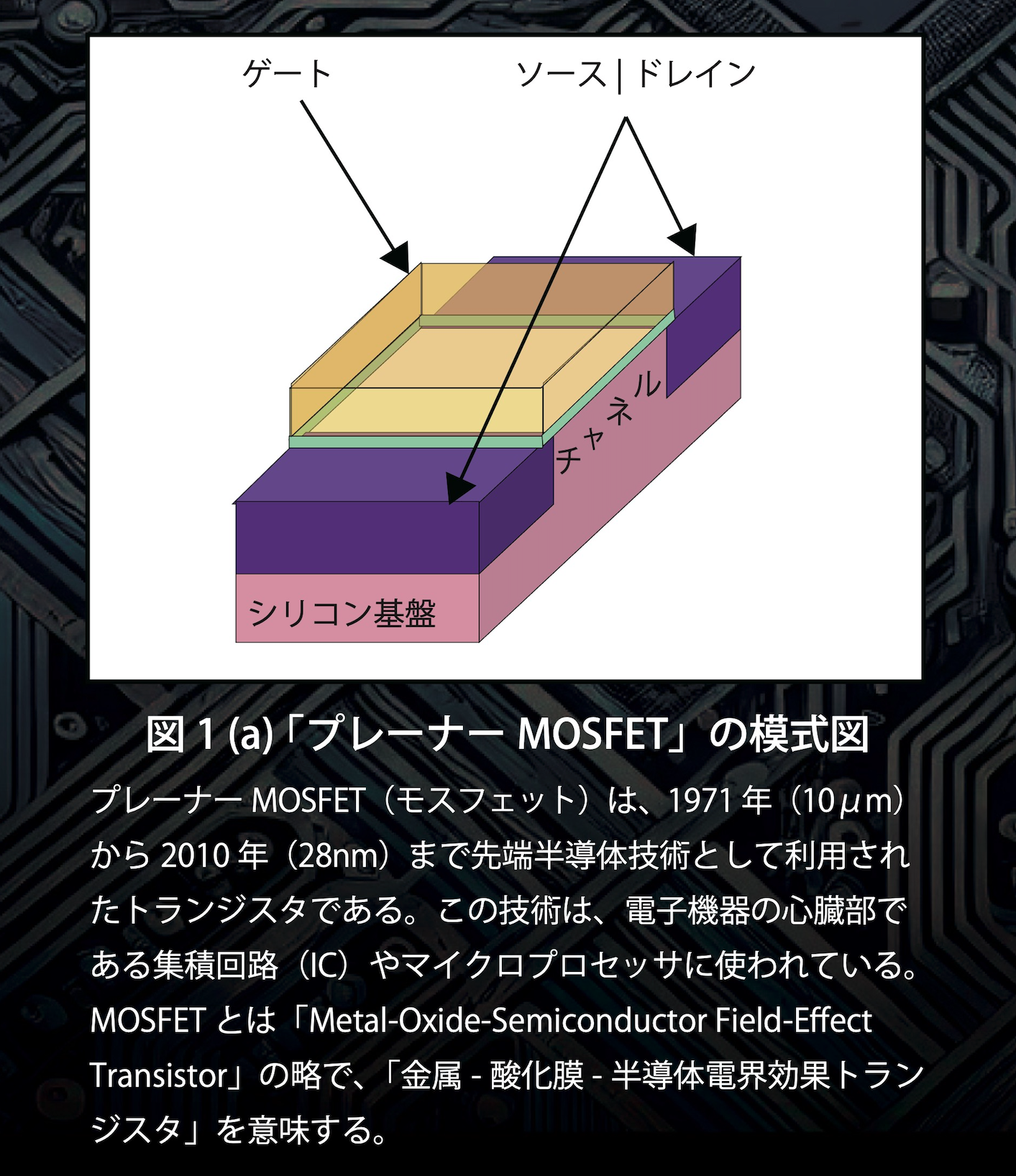
1.2 65-year history of MOSFET (metal-oxide-semiconductor) 4
1.2.1 Japanese companies withdraw from the development race with planar MOSFET 6
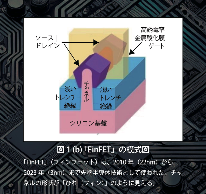
1.2.2 FinFET deployment goes global 8
1.2.3 FinFET developed from the idea of Japanese engineers 9
1.2.4 Japanese engineers who followed FinFET (2014) 10
1.2.5 Transition to GAA (Gate-All-Around) at 2nm (2024) 11
1.2.6 Is the transition from FinFET to GAA an evolution rather than a revolution? 12
1.3 “Next-generation technologies” associated with the 2nm process 15
1.3.1 Improved performance and area with backside power supply (BSPD) 16
1.3.2 Through-silicon via (TSV) 17
1.3.3 Intel has already completed backside power supply at 2nm 18
1.3.4 Intel also discloses backside power supply wafer manufacturing method 19
1.3.5 Intel expects backside power supply will not increase costs 20
1.3.6 2nm front-side power delivery (FSPD) sees increased use of EUV 20
1.3.7 Intel says backside power delivery will not degrade yields 21
1.3.8 Through-silicon vertical electrical interconnects are needed for 3D stacking 21
1.3.9 Interposers are essential for 2.5D stacking 22
1.3.10 Intel and AMD develop their own chiplets 22
1.3.11 Intel’s proprietary chiplet technology “Foveros” 23
1.3.12 AMD also develops its own chiplet technology 25
1.3.13 Chiplet technology at NVIDIA 28
1.3.14 Chiplet interoperability and standardization 30
1.3.15 UCIe (Universal Chiplet Interconnect Express) 31
1.3.16 AIB: Advanced Interface Bus (2018) 32
1.3.17 The 10 companies that dominate the Die-to-Die (D2D) standard 33
1.3.18 The business of selling chiplets 35
1.3.19 Alpha Wave Semi’s chiplet business 36
1.3.20 3D and 2.5D stacking and backside power 36
1.3.21 Extreme ultraviolet lithography (EUV) at advanced nodes 37
1.4 TSMC’s status for the 2nm node and beyond 40
1.4.1 TSMC’s EUV adoption status 40
1.4.2 TSMC’s 2nm and beyond roadmap: 41
1.5 Samsung 2nm roadmap 43
1.6 Intel’s 2nm roadmap 45
1.7 Rapidus’ 2nm fab 47
1.7.1 The significance of Japan having a next-generation semiconductor fab 47
1.7.2 Rapidus’ 2nm schedule 48
1.7.3 Is Rapidus’ 2nm schedule slow? 48
1.8 Eight major business types that make up the semiconductor supply chain 50
1.8.1 EDA (Electronic Design Automation) companies? 50
1.8.2 IP (Intellectual Property) providers 50
1.8.3 Fabless semiconductor companies 51
1.8.4 Semiconductor manufacturing companies (foundries) 51
1.8.5 IDM (Integrated Device Manufacturers) 51
1.8.6 OSAT (Outsourced Semiconductor Assembly and Test) 52
1.8.7 Semiconductor material suppliers 53
1.8.8 Semiconductor manufacturing equipment manufacturers 53
1.9 Overview of Japan’s semiconductor strategy 54
1.9.1 Strengthening the semiconductor manufacturing base 54
1.9.2 Stimulating the local economy with the entry of semiconductor-related companies and job creation: 54
1.9.3 Quantitative targets for semiconductor revival (achieving 15 trillion yen in sales in 2030) 55
1.9.4 Supplementary budget for semiconductors 56
1.9.5 Enforcement of new laws and huge investments: measures to strengthen domestic semiconductor fabs 57
1.9.6 Establishment of a new tax system to promote production in the domestic semiconductor industry 60
1.10 Global semiconductor competition 61
1.10.1 Initiatives of major countries 61
1.10.2 Securing next-generation semiconductors 62
1.10.3 Initiatives for manufacturing next-generation logic and memory semiconductors 62
1.10.4 Establishment of a cutting-edge semiconductor manufacturing ecosystem 63
1.10.5 Lapidus Corporation 66
1.10.6 Additional support for Rapidus 67
1.10.7 Rapidus’ future business phase and support 69
1.10.8 Semiconductor technology for the Beyond 2nm generation 70
1.10.9 The world’s first investment support for cutting-edge semiconductors 72
1.11 Developing use cases for next-generation semiconductors 73
1.11.1 Hierarchical structure of services in AI and computing 73
1.11.2 Memory and storage strategy 74
1.11.3 The direction of memory for AI calculations 75
1.11.4 Recent efforts toward realizing next-generation semiconductors 77
1.11.5 Rapidus West Coast base (Rapidus Design Solutions) 78
1.11.6 Collaboration with Tenstorrent and Esperanto 79
1.11.7 Why are chiplets necessary for next-generation semiconductors? 80
1.11.8 The importance of and efforts in advanced packaging strategies 82
1.11.9 Development of advanced packaging technology for advanced semiconductor back-end processing 83
1.12 Leading-Edge Semiconductor Technology Center (LSTC) 85
1.12.1 Organization of Leading-Edge Semiconductor Technology Center (LSTC) 85
1.12.2 Research and development projects of LSTC 86
1.13 Diplomatic benefits of advanced semiconductors 88
1.13.1 Industrial support for legacy semiconductors and economic security 88
1.13.2 Survey on legacy semiconductors in the United States 88
1.13.3 Ensuring security in semiconductor-related industries 89
1.13.4 Risks of technology and data leakage and countermeasures 90
1.13.5 International semiconductor cooperation 91
1.13.6 Japan-U.S. Summit and Japan-U.S.-Philippines Summit 93
1.13.7 3rd Japan-U.S. Commercial and Industrial Partners (JUCIP) Meeting 94
1.13.8 Semiconductor cooperation between Japan and the EU 95 1.13.9 Semiconductor cooperation between Japan and the UK 96
1.13.10 Semiconductor cooperation between Japan and the Netherlands 97
1.13.11 Overview of R&D support systems in the US and EU 98
1.14 Financial sustainability of Japan’s semiconductor strategy 100
1.14.1 Contents of the Financial System Subcommittee (held on April 9, 2024) 100
1.14.2 Scale of semiconductor support measures in each country (reflecting tax systems and the latest situation) 101
1.15 Semiconductor strategies of countries around the world 102
1.15.1 Semiconductor support projects in the US 102
1.15.2 TSMC overseas investment and government support: a comparison of countries 104
1.16 Power demand and semiconductors 106
1.16.1 Power demand for data centers 106
1.16.2 Attracting AI data centers (DCs) and energy measures 107
1.16.3 AI data center initiatives by general power transmission and distribution companies 110
1.16.4 GX Green Transformation Executive Committee 111
1.16.5 Energy supply to support AI and data centers 112
1.16.6 AI data centers and advanced computing resources 113
1.16.7 Optimization of AI computing infrastructure and power consumption management 115
1.17 Semiconductor human resource development 118
1.17.1 Establishment of advanced semiconductor development and human resource development centers 118
1.17.2 Strengthening research and development and human resource development through LSTC activities 119
1.17.3 Collaboration with overseas institutions and human resource development 120
1.17.4 Initiatives related to semiconductor human resource development 121
1.17.5 Semiconductor human resource development efforts in the Tohoku region 122
1.17.6 The importance of highly skilled human resource development and specific efforts 122
1.17.7 Strengthening the supply chain of semiconductor materials 123
1.17.8 LSTC Human Resource Development Working Group (WG) 124
1.17.9 Regional consortium to promote semiconductor human resource development 126
1.18 Economic ripple effects on the local community 127
1.18.1 Economic ripple effects on Kumamoto Prefecture 127
1.18.2 Semiconductor-related companies’ entry into and investment in Kumamoto Prefecture 128
1.18.3 Prime Minister Kishida, TSMC, and local companies roundtable 129
1.18.4 Supporting semiconductor supply chain resilience with the Economic Security Fund 130
1.19 Sources 134
2. NVIDIA’s history: 30 years of trials, challenges, and success 135
2.1 Trends in NVIDIA sales 135
2.2 Market share of desktop PC GPU cards by company 139
2.3 NVIDIA AI semiconductors for data centers 140
2.4 References 141
2.5 Collaboration between NVIDIA and Taiwanese semiconductor manufacturing: Success built through cooperation 143
2.5.1 1960s Challenges and changes starting from back-end processing 143
2.5.2 1970s Introduction of front-end technology and application-centered business strategy 144
2.5.3 1980s Pure-play foundries that changed the semiconductor industry 148
2.5.4 Growth of TSMC 151
2.5.5 Taiwan’s semiconductor manufacturing industry and NVIDIA 153
2.5.6 References 154
3. Graphics and AI revolution: Jensen Huang and NVIDIA Challenges 155
3.1 NVIDIA and Jensen Huang 155
3.2 NVIDIA Founded 156
3.2.1 NVIDIA Founded (1993) 156
3.2.2 Jensen Huang (Huáng Rénxūn) 156
3.2.3 Co-founders 159
3.3 The Early Days of NVIDIA (1993) 168
3.3.1 Origin of the NVIDIA Name 168
3.3.2 3D Graphics Technology at the Time of NVIDIA’s Founding 171
3.4 First Product: NV1 175
3.4.1 Manufacturing Partnership with STMicro (1995) 175
3.4.2 Microsoft DirectX (1995) 180
3.4.3 For Sega NV2 (1995) 180
3.4.4 Quiet Pivot (1996) 181
3.4.5 Cut 50% of staff 182
3.4.6 Closed cafeteria but continued nightly pizza orders 186
3.4.7 NV1 returns piled up to create a monument 187
3.4.8 NVIDIA returns to stealth and restarts 189
3.4.9 Sega’s in-house next-generation Game Development Contest (1996) 191
3.4.10 11 people from Sega of America transfer to Hitachi (1996) 194
3.4.11 What happened to 3dFx (1996) 194
3.4.12 Aftermath of “Black Belt” vs. “.Katana” (1996) 195
3.4.13 “Bubble Economy” (1992) and “Independent Enterprise Principle” (1994) 196
3.4.14 $7 million MOU written on a napkin (1996) 197
3.4.15 Amicable termination of NV2 development contract with Sega (1997) 199
3.4.16 Dreamcast goes to Imagination (1997) 200
3.4.17 Hitachi Semiconductor faces financial difficulties due to sudden changes in the DRAM market (1996) 201
3.5 From 3D accelerators to GPUs (NV3-NV20) 201
3.5.1 Microsoft promotes DirectX (September 1995) 201
3.5.2 TSMC from NVIDIA’s perspective (1996) 205
3.5.3 NV3: Gained 10-15% market share with RIVA 128 (1997) 207
3.5.4 NV10: GeForce 256 (1999) named GPU 209
3.5.5 GPU driver source not disclosed (1999) 213
3.5.6 Programmable GPU: NV20: GeForce 3 (2001) 214
3.6 NVIDIA’s OS development 217
3.6.1 Size of NVIDIA’s OS development team 218
3.6.2 Why is NVIDIA so keen on OS development? 218
3.6.3 Are 99% of blue screens caused by NVIDIA drivers? 221
3.6.4 Graphics benchmarks in 2000 223
3.7 NVIDIA’s financials 223
3.7.1 Jensen’s shareholding at NVIDIA’s IPO 224
3.7.2 Debt-free management 224 3.7.3 NVIDIA’s largest shareholders 225
3.8 2000s: Diversification and market dominance 226
3.8.1 Expansion into new markets: data centers, automotive, etc. 226
3.8.2 Major new product generation launches and technology advances 231
3.9 Gaining technological advantage through acquisitions 234
3.9.1 Acquisition of 3dfx Interactive (2000) 234
3.9.2 Acquisition of MediaQ and Tegra series (2003) 235
3.10 Strategic partnerships 237
3.10.1 Sony Playstation 3 (2000s) 237
3.10.2 Microsoft Xbox 360 (2000s) 238
3.10.3 IBM HPC High performance computing (2000s) 238
3.10.4 Audi Google Earth navigation (2000s) 238
3.10.5 NVIDIA orders 20 SH7786 evaluation boards from Hitachi 240
3.10.6 Tesla Motors (2000s) 243
3.11 AI Steady business expansion behind the scenes of the revolution 243
3.11.1 The advent of AI deep learning 243
3.11.2 NVIDIA GPUs become essential for AI research and development 245
3.11.3 NVIDIA GPUs and CUDA democratize AI development 246
3.11.4 Impact on the industry 247
3.12 CUDA platform 247
3.12.1 Popularization of large-scale parallel computing with CUDA 248
3.12.2 CUDA parallel computing model 249
3.12.3 Support for processing order and data dependency 249
3.12.4 How parallel processing works in CUDA 249
3.12.5 Memory hierarchy and data transfer 250
3.12.6 CUDA library (parallel computing software stack): 251
3.12.7 CUDA’s contribution to computer science 252
3.12.8 CUDA gives AI researchers wings 253
3.12.9 CUDA transforms industries: from genomics to robotics 254
3.13 The beginning of CUDA: Cg, the C language for graphics 254
3.13.1 What is a programmable shader? 255
3.13.2 The history of programmable shaders 255
3.13.3 NVIDIA’s development of its own shader compiler 256
3.13.4 Market response to NVIDIA’s shader compiler Cg 257
3.13.5 The origin of the word “CUDA” 259
3.13.6 The quantum leap from Cg to “CUDA” 260
3.13.7 GPU Development tool “CUDA Toolkit” 261
3.13.8 CUDA debugging tool NVIDIA Nsight 262
3.13.9 GPU documentation and support 262
3.14 Is software a “service that only generates losses” for chip companies? 263
3.14.1 Early Jensen’s view of software 263
3.14.2 Jensen’s critique of the “SH franchise” 264
3.14.3 What NVIDIA learned from “NV1” at the time 265
3.14.4 Initial opposition to expanding Cg compiler development staff (2003) 266
3.14.5 Engineers’ feelings after the IPO (2003) 267
3.14.6 Linus, Stallman, and open source 267
3.14.7 From NVIDIA to Windows OS 269
3.14.8 Talented engineers from NVIDIA 270
3.14.9 A young Cg compiler engineer struggling alone (2002) 271
3.14.10 Conditions for being called a general-purpose GPU 273
3.14.11 Appealing the ease of GPU programming with CUDA 273
3.14.12 References 274
3.15 Mobilizing researchers to promote NVIDIA 274
3.15.1 Optimizing Google TensorFlow for NVIDIA 274
3.15.2 Integrating Google Cloud 275
3.15.3 Providing GPU services from Amazon Web Services (AWS) 275
3.15.4 Accelerating AI research with Amazon Machine Images (AMI) 275
3.15.5 Microsoft: Azure Machine 275
3.15.6 AI research collaboration with universities 276
3.16 NVIDIA’s cutting-edge AI chip architecture 277
3.16.1 The direction of NVIDIA GPU architecture 277
3.16.2 History of NVIDIA GPU architecture 278
3.16.3 Linking GPU architecture with CUDA 279
3.17 Tensor Core 280
3.17.1 Acceleration of matrix operations 281
3.17.2 Implementation of matrix multiplication (Fused Multiply-Add, FMA) 282
3.17.3 Support for multi-precision operations 282
3.17.4 Collaboration with the Transformer Engine 283
3.17.5 Application areas where Tensor Core is useful 283
3.18 Hopper architecture 284
3.18.1 Features of the Hopper architecture 284
3.19 Transformer engine 285
3.19.1 Background of the Transformer architecture 285
3.19.2 Details of the Transformer engine 285
3.19.3 Applications of the Transformer engine 286
3.20 Dynamic programming (DP) 287
3.21 Simultaneous execution of multiple tasks with MIG (Multi-Instance GPU) 287
3.22 NVLink 4.0 speeds up GPU-GPU-CPU transfers 288
3.23 HBM3 memory (High Bandwidth Memory 3) 288
3.24 AI chips that challenge NVIDIA 290
3.24.1 “The AI Warring States Period will begin in 2025” 290
3.24.2 Major IT companies enter the race with their own AI chips 291
3.24.3 AMD pursues CUDA with RDNA and ROCm 291
3.24.4 Intel competes by acquiring Ponte Vecchio, Gaudi, and Mobileye 295
3.24.5 Google replaces NV with cloud AI using TPU 300
3.24.6 Tesla develops self-driving AI chip Full Self-Driving in-house 300
3.24.7 Amazon develops AI chips Trainium and Inferencia in-house 301
3.24.8 Qualcomm challenges with mobile and in-vehicle AI chips 301
3.24.9 Apple challenges NVIDIA with M-series built-in GPU 302
3.24.10 Tenstorrent’s “Grayskull” and “Wormhole” 302
3.24.11 Graphcore’s Intelligence Processing Unit 303
3.24.12 Cerebras Systems’ Wafer Scale Engine 303
3.24.13 SambaNova’s Reconfigurable Dataflow Unit 304
3.24.14 Mythic AI’s Analog AI Inference Chip 305
3.24.15 Groc’s Tensor Streaming Processor 305
3.24.16 NVIDIA Challengers Roundup 306
3.25 NVIDIA Innovations Start Transforming Industries 307
3.25.1 Healthcare and Life Sciences 307
3.25.2 Autonomous Vehicles and Transportation 308
3.25.3 Manufacturing and robotics 309
3.25.4 Finance and banking 309
3.25.5 Financial risk management and compliance applications 310
3.25.6 Media and entertainment 310
3.26 References 311
3.27 Conclusion 311
3.28 Musings 311
4. Arm’s new strategy: TSMC-optimized IP improves performance, efficiency, and area 315
4.1 Trends in Arm revenue and shipments 315
4.2 Expansion of Flexible Access 315
4.3 Evolution of embedded Arm architecture and IP 317
4.4 Examples of embedded chip products 320
4.5 Compute subsystems are for specific foundries 320
4.6 References 321
5. TSMC’s 24 Annual: Sales trends and technology node changes 323
5.1 TSMC sales trends 323
5.2 Profits and profit margins 326
5.3 References 327
6. Design a RISC-V Prototype using Google-funded shuttle for DARPA automated design flow 329
6.1 Realizing MARMOT RISC-V with 1MB+ memory 330
6.2 Good fortune comes with Google free shuttle 331
6.3 Efabless Caravel Harness 332
6.4 Linux-based IoT edge and RTOS-based IoT edge 333
6.5 Open Road work log (2022) 333
6.6 Software verification of Efabless prototype chip (2024) 335
6.7 MPW-6 demo (August 1, 2024, November 20) 338
6.8 “JASA1 chip evaluation board” for distribution to members (planning stage) 339
6.8.1 Cost image of “JASA1 chip evaluation board” 340
6.8.2 Initialization of Dual and Quad connections with QPI flash (completed) 341
6.8.3 Evaluation of QPI flash direct execution performance on actual equipment (in progress) 342
6.8.4 Release of Chisel source code (in progress) 342
6.8.5 Direct execution from QPI flash via cache 344
6.8.6 MPW-7 Marmot can operate at high speed of 50MHz 344
6.8.7 Chisel verification with logic simulation and FPGA 344
6.8.8 MPW-7 Marmot’s PSRAM direct execution function added to JASA1 345
6.9 Chisel study group 346
6.9.1 “Starting digital circuit design with Chisel” 346
6.9.2 Verification of Chisel operation on Arty A7 FPGA 347
6.10 Future Plans 347
6.11 MPW-8 Releases Self-Developed SH-2 348
6.12 Impressions 349
6.13 Conclusion 349
6.14 Acknowledgements 349
7. Andes Growing with RISC-V: The Future of Taiwan’s No. 1 IP Company 351
7.1 Andes Technology with 30% RISC-V Market Share 351
7.2 CPU IP Lineup and Strategy for 2030 354
7.3 Vision for 2030 361
7.4 References 363
8. Scalable RISC-V for DX provided by Tenstorrent 365
9. From Simple Microcontrollers to Complex Multi-Core SoCs
– Debugging RISC-V-Based Chips Made Easy391
10. RISC-V and the US-China conflict: Open source cooperation continues beyond the divide 401
10.1 Introduction 401
10.2 Origin and basic features of RISC-V 401
10.2.1 What is instruction set architecture, ISA? 402
10.2.2 Strategic benefits to companies that control the “instruction set” 404
10.2.3 Why RISC-V emerged 404
10.2.4 Why Google is supporting RISC-V on a large scale 405
10.2.5 40-year history of the “RISC instruction set” at the University of California, Berkeley 406
10.2.6 Differences between RISC-V’s business model and Arm’s 408
10.2.7 IP revenue and number of design starts surpass Arm (2023) 409
10.2.8 Arm leads RISC-V in fundraising through IPO 410
10.2.9 Arm withdraws request for Apple license fee increase 411
10.2.10 Performance comparison of cutting-edge RISC-V and cutting-edge Arm 412
10.2.11 Google and Qualcomm team up to complete Android for RISC-V, China also uses it 413
10.2.12 Bosch, Qualcomm, and Infineon’s in-vehicle RISC-V IP 415
10.3 More than 300 companies in China use RISC-V to develop products 416
10.3.1 T-Head (Pingtouge) RISC-V “Xuantie” (Xuantie) 417
10.3.2 Alibaba “Xuantie” RISC-V system 418
10.3.3 HiSilicon RISC-V “Hi3861” 418
10.3.4 Huawei Hi3861 RISC-V ecosystem 419
10.3.5 StarFive’s RISC-V JH7110 SoC 421
10.3.6 China’s Terapines provides software-hardware co-design environment 422
10.3.7 Chinese Academy of Sciences “XiangShan” open RISC-V 423
10.4 Superchip embargo to China and RISC-V 424
10.4.1 US export restrictions on digital semiconductor technology to China 424
10.4.2 Japan’s response to export restrictions 424
10.4.3 2023 Europe China and Taiwan talk at RISC-V summit 426
10.4.4 US Congressman requests RISC-V export restrictions to Biden administration 426
10.4.5 Export restrictions on open industrial standards are difficult 427
10.4.6 The possibility of export restrictions on RISC-V cannot be denied 428
10.5 Japan’s semiconductor policy regarding RISC-V 429
10.5.1 METI-led RISC-V subsidy program 2018-2023 429
10.5.2 Confirmation of Japan-US economic security and technical cooperation at APEC2023 429
10.5.3 Japan-US small reactor (SMR) cooperation announced immediately after APEC 2023 430
10.6 Rapidus Creation as an integrated policy of the Japanese government 431
10.6.1 Integrating foreign policy, security policy, and economic policy 432
10.6.2 Strategic partnership between Lapidus and Tenstorrent 433
10.6.3 Expectations of the Japanese and US governments for Lapidus 434
10.6.4 Development of civilian and military dual-use manufacturing technology 435
10.6.5 NVIDIA manufactures military and civilian dual-use AI chips 436
10.6.6 Partnership between Lapidus and RISC-V CPU and AI chip companies 437
10.6.7 Partnership between Lapidus and Arm user semiconductor manufacturers 438
10.7 RISC-V’s footprint in the semiconductor industry 439

